Download
1 / 37
400 likes | 624 Views
Explore the function and design of counters and registers in sequential logic circuits, including various types like BCD counters and shift registers.

E N D
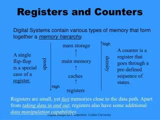
Counters • A counter circuit is a sequential logic circuit used to count number of clock pulses received. • Counters are constructed by a number of Flip- flops connected in cascade. • Counters are a very widely used component in digital circuits , and are manufactured as separate ICs and also incorporated as parts of larger integrated circuits. 241-208 CH9
Classification • Asynchronous (ripple) counter – changing state bits are used as clocks to subsequent state flip-flops • Synchronous counter – all state bits change under control of a single clock (All F/F change state simultaneously) • Decade counter – counts through ten states per stage • Up/down counter – counts both up and down, under command of a control input • Ring counter – formed by a shift register with feedback connection in a ring • Johnson counter – a twisted ring counter • Cascadedcounter and • Modulus counter.
Assignment 2 • Working of a 4 bit ripple counter and Up/Dn counter • Synchronous counter design using T F/F for the following states 0 8 12 14 15 7 3 1 0 241-208 CH9
BCD Counter State Diagram 241-208 CH9
A decade counter has four flip-flops and 16 potential states, of which only 10 are used and if we connected a series of counters together we could counter to 100 or 1,000 or what ever number we wanted. • The total number of counts that a counter can count too is called its MODULUS. A counter that returns to zero after n counts is called a modulo-n counter, for example a modulo-8 (MOD-8), or modulo-16 (MOD-16) counter, etc, and for an “n-bit counter”, the full range of the count is from 0 to 2n - 1 241-208
BCD • Count sequence from 0000 (“0”) through to 1001 (“9”) is called a binary-coded-decimal counter or BCD Counter or MOD-10 counter can be constructed using a minimum of four toggle flip-flops. 241-208 CH9
The 74LS90 BCD Counter • The 74LS90 integrated circuit is basically a MOD-10 decade counter that produces a BCD output code. • The 74LS90 consists of four master-slave JK flip-flops internally connected to provide a MOD-2 (count-to-2) counter and a MOD-5 (count-to-5) counter. • The 74LS90 has one independent toggle JK flip-flop ( 2) driven by the CLK A input and three toggle JK flip-flops that form an asynchronous counter ( 5) driven by the CLK B input as shown. 241-208 CH9
7490 241-208 CH9
The 74LS90 counter consists of a divide-by-2 counter and a divide-by-5 counter within the same package. • We can use either counter to produce a divide-by-2 frequency counter only, a divide-by-5 frequency counter only or the two together to produce our desired divide-by- 10 BCD counter. 241-208 CH9
2 counter With the four flip-flops making up the divide-by-5 counter section disabled, if a clock signal is applied to input pin 14 (CLKA) and the output taken from pin 12 (QA), we can produce a standard divide-by-2 binary counter for use in frequency dividing circuits as shown. 241-208 CH9
5 counter 241-208 CH9
10 Counter • To produce a divide-by-10 BCD decade counter, both internal counter circuits are used giving a 2 times 5 divide-by value. Since the first output QA from flip-flop A is not internally connected to the succeeding stages, the counter can be extended to form a 4-bit BCD counter by connecting this QA output to the CLKB input as shown. 241-208 CH9
Decoder Driver 241-208 CH9
4-bit BCD Counter Circuit 241-208 CH9
Application of counters • Frequency counters • Digital clock • Time measurement • A to D converter • Frequency divider circuits • Digital triangular wave generator. 241-208 CH9
Shift Registers • Shift registers are a type of sequential logic circuit, mainly for storage of digital data. ( 0s and 1s) • To store a single bit one F/F is required. • To store n bits of information n F/F are required • They are a group of flip-flops connected in a chain so that the output from one flip-flop becomes the input of the next flip-flop. • All the flip-flops are driven by a common clock, and all are set or reset simultaneously.
Types • Serial In/Serial Out Shift Registers • Serial In/Parallel Out Shift Registers • Parallel In/Serial Out Shift Registers • Parallel Out/Parallel Out Shift Registers • Bidirectional Shift Registers • Special Shift Counters Ring Counters and Johnson Counter 241-208 CH9
Basic Shift Register Functions • A shift register is an arrangement of flip-flops with important applications in storage and movement of data. Data in Data in Data out Data out Data in Serial in/shift right/serial out Serial in/shift left/serial out Parallel in/serial out Data out Data in Data in Data out Data out Rotate right Rotate left Serial in/parallel out Parallel in/parallel out
1 1 1 1 1 CLK Serial-in/Serial out Shift Register • 5-bit serial in/serial out shift register implemented with D flip-flops. 1 241-208 CH9
CLK CLK CLK CLK Serial In/Parallel Out Shift Registers • 4-bit serial in/parallel out shift register • For example, assume the binary number 1011 is loaded sequentially, one bit at each clock pulse. 241-208 CH9
The 74HC164A Shift Register • 8-bit serial in/parallel out shift register • One of the two serial data inputs may be used as an active HIGH enable to gate the other input. • If no enable is needed, the other serial input can be connected to Vcc. • The 74HC164A has an active LOW asynchronous clear. • Data is entered on the leading-edge of the clock. CLR CLK A Serial inputs B Q3 Q0 Q1 Q2 Q4 Q5 Q6 Q7
Parallel In/Serial Out Shift Registers • Shift registers can be used to convert parallel data to serial form. D2 D3 D0 D1 SHIFT/LOAD Serial data out Q3 Q0 Q1 Q2 CLK
The 74HC165 Shift Register • 8-bit parallel in/serial out shift register • The clock (CLK) and clock inhibit (CLK INH) lines are connected to a common OR gate, so either of these inputs can be used as an active-LOW clock enable with the other as the clock input. • Data is loaded asynchronously when SH/LD is LOW and moved through the register synchronously when SH/LD is HIGH and a rising clock pulse occurs. D0 D1 D2 D3 D4 D5 D6 D7 Q7 SH/LD SER CLK INH Q7 CLK
Parallel In/Parallel Out Shift Registers 241-208 CH9
Bidirectional Shift Register • Bidirectional shift registers can shift the data in either direction using a RIGHT/LEFT input. 241-208 CH9
Shift Register Counters • Shift registers can form useful counters by recirculating a pattern of 0’s and 1’s. Two important shift register counters are the Johnson counter and the ring counter. • The Ring counter and Johnson counter can be made with a series of either D flip-flops or J-K flip-flops. 241-208 CH9
Ring Counter • The ring counter can also be implemented with either D flip-flops or J-K flip-flops. • 4-bit ring counters are constructed from a series of D flip-flops J-K flip-flops. Notice the feedback. Initial status after clear and Preset Q0 Q1 Q2 Q3 0 0 0 1
Ring Counter • A common pattern for a ring counter is to load it with a single 1 or a single 0. • Draw the waveforms for the 4-bit ring counter ( shown in the previous slide) 241-208 CH9
Johnson counter • The Johnson counter is useful when you need a sequence that changes by only one bit at a time but it has a limited number of states (2n, where n = number of stages). The first five counts for a 4-bit Johnson counter that is initially cleared are:CLK Q0Q1Q2Q3 0 1 2 3 4 5 6 7 0 0 0 0 1 0 0 0 1 1 0 0 1 1 1 0 1 1 1 1 0 1 1 1 0 0 1 1 0 0 0 1 What are the remaining 3 states?
A Johnson counter is also known as switch-tail ring counter, twisted ring counter, walking ring counter, or Möbius counter . It is is a modified ring counter, where the output from the last stage is inverted and fed back as input to the first stage. The register cycles through a sequence of bit-patterns, whose length is equal to twice the length of the shift register, continuing indefinitely. These counters are useful in digital-to-analog conversion, generating control signals etc.
In order to follow an ideal sequence of states both the Ring and the Johnson counter must initially be forced into a valid state in the count sequence using preset and clear inputs. 241-208 CH9
Shift Register Applications • Examples: Time Delay, Parallel/Serial Data Converter, and Keyboard Encoder An 8-bit serial in/serial out shift register has a 40 MHz clock. What is the total delay through the register? The delay for each clock is 1/40 MHz = 25 ns 25 ns The total delay is 8 x 25 ns =200 ns = 200 ns
Serial data transfer • One application of shift registers is converting between “serial data” and “parallel data” • Computers typically work with multiple-bit quantities • ASCII text characters are 8 bits long • Integers, single-precision floating-point numbers, and screen pixels are up to 32 bits long • But sometimes it’s necessary to send or receive data serially, or one bit at a time. Some examples include: • Input devices such as keyboards and mice • Output devices like printers • Any serial port, USB or Firewire device transfers data serially
serial device computer Receiving serial data • To receive serial data using a shift register: • The serial device is connected to the register’s SI input • The shift register outputs Q3-Q0 are connected to the computer • The serial device transmits one bit of data per clock cycle • These bits go into the SI input of the shift register • After four clock cycles, the shift register will hold a four-bit word • The computer then reads all four bits at once from the Q3-Q0 outputs.
computer serial device Sending data serially • To send data serially with a shift register, • The CPU is connected to the register’s D inputs • The shift output (Q3 in this case) is connected to the serial device • The computer first stores a four-bit word in the register, in one cycle • The serial device can then read the shift output • One bit appears on Q3 on each clock cycle • After four cycles, the entire four-bit word will have been sent