Download
1 / 17
170 likes | 312 Views
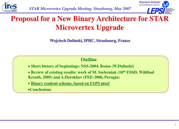
Proposal for a New Binary Architecture for STAR Microvertex Upgrade. Wojciech Dulinski, IPHC, Strasbourg, France. Outline Short history of beginnings: NSS-2004, Roma (W.Dulinski)

E N D
Proposal for a New Binary Architecture for STAR Microvertex Upgrade Wojciech Dulinski, IPHC, Strasbourg, France • Outline • Short history of beginnings: NSS-2004, Roma (W.Dulinski) • Review of existing results: work of M. Szelezniak (10th ESSD, Wildbad Kreuth, 2005) and A.Dorokhov (FEE-2006, Perugia) • Binary readout scheme, based on FAPS pixel • Conclusions
S1 vbias AVDD Read pwr_on output1 Cs1 S2 AVDD x(5-10) Read output2 Cs2 gnd output1 General pixel architectureand readout pattern BUF output2 clk S1 INTEGRATION S2 pwr_on read Analog CDS on pixel using analog memories for storing two successive frames : possible way to limit the integration time, effective use of a trigger - Slow integration clock (1MHz 640 µs integration time): low dissipation, comfortable stabilisation time of the on-pixel amplifier after Power_On - Readout of all pixels after trigger only: no need for perfect internal readout chain compensation - External compensation, global correction (common mode) possible: limited risk for experimental “unknown” factors - Lower signal amplitude dispersion: less power, smaller digitisation precision required (~8bits) READOUT
First test results from Mimosa9 test structures Pixel_1: 400 fF Fe55 5.9 keV peak Time scale: 10s/sq. RMSNoise < 8 ADCENC = 16-20 e- Storage capacitor discharge time of a (600 mV) pulse is more than comfortable. What after irradiation? Very preliminary!!!
Conclusions 2: STAR application- Increase of a dark current after irradiation is THE critical factor, in order to run detector at room temperature (not well controlled) AND using several milliseconds integration time- Each process and each layout should be carefully studied for this effect AND compared to STAR radiation environment - Going to shorter integration time (order of magnitude) and systematic research on the more radiation-tollerant layout techniques is strongly recommended, in order to have necessary safety factor for the experiment “unforeseen”- CDS on pixel using analog memory for two frames storing scheme seems promising, but still requires deeper understanding (new small prototypes)
Gain Gain DC coupled and AC coupled on-pixel amplifiers AC coupled amp: • Separation from power supply of the sensing node • Increase of the voltage increase of the depleted region no change on the operating point • Separation from influence of the leakage current • Increase of the leakage current after irradiation change of the bias on the sensing node no change on the OP DC coupled Compact implementation AC coupled
DC versus AC diode coupling Charge collection efficiency and ENC in function of bias of charge collecting diode DC seems to win in simplicity and performance…
Amplifiers for MAPS Amplification is needed to decrease noise contribution from switching networks, like clamping or sampling. • PMOS transistors not allowed inside pixel -> signal decrease due to parasitic NWELL • but using PMOS transistor as a load would be the preferred choice to increase in-pixel amplifier gain… load bias gate reset out bias in in out vb cascode signal current in
Amplifiers for MAPS small signal Gain = Vout/Vin = gm1 /(gm2 +gmb2 +gds1 +gds2) M2 bias As an example from simulation to be presented later: gm1=47 mS gm2=4 mS gmb2=0.9 mS gds1=8 nS gds2=0.5 mS out • gds1 and gds2 <<gm1,gm2 , gmb2 • so one need to increase gm1and decrease gm2 and gmb2 • with decreasing gm2 we decrease DC current, and hence gm1 so there is a limiting contradiction for the gain/bandwidth of this schematic… Id in M1 signal current Due to gm2 there is unwanted dependency of Id on Uout , so can we reduce dependency of Id on Uout without changing gm2 ? ?
Improved load for the common source transistor -> decouple the gate of the load transistor from the power supply with one additional NMOS transistor, used as a diode • due to the floating gate and parasitic gate-to-source capacitive coupling the AC voltage at the gate will follow to the output AC voltage -> • AC current and hence the load for the common source transistor decreases • load for DC is almost unchanged as DC voltage drop on additional NMOS transistor is small M3 M2 gate out bias in M1 signal current Gain = Vout/Vin = gm1 /(gm2 +gmb2 +gds1 +gds2) The AC gain should increase, while the DC operational point should not change!
Test structures with new amplifier implemented in Mimosa15 chip improved load with power on switch low frequency-pass feedback correlated double sampling circuit common source transistor with power on switch NWELL diode NWELL size is4.25 mm x 3.4 mm, pixel pitch size 30 mm x 30 mm, pixel matrix: 4 columns x 15 rows
Summary (VI-th Front End Electronics Workshop, Perugia, 2006) • new resistive AC load, which uses only NMOS transistors, is proposed • NMOS based amplifier using new type of load and feedback is designed and simulated • the gain increases by factor of 2 in comparison to the gain of existing amplifier schematics, which use only NMOS transistors • in comparison to old schematic, the same gain can be achieved with smaller power consumption • the designed amplifier implemented in MAPS using AMS0.35 OPTO process and tested with Fe55 source • the tested MAPS has the following measured properties: • low noise, ~7.5 e (after CDS), and hence higher signal-to-noise ratio • conversion gain is about 74 mV/e • gain variation due to process variation is about 2 % • charge collection in seed pixel is 18 % • charge collection in the cluster 3x3 is 58 % • the amplifier can be also used in schematics, where one need to save the space, cause it does not contain PMOS transistors (and hence PWELLs)
Mimosa8 (TSMC-0.25µ, 8 µm epi) – a binary readout demonstrator • CDS in pixel, based on “clamping” circuit solution • On-chip FPN suppression • Offset compensated comparator at the end of each column • Pixel pitch 25 x 25 µm2 Prototype in collaboration with Dapnia/Saclay
Mimosa8 beam tests results Comparator voltage scan (all pixels) • Output noise: 0.9 mV (ENC = 15 electrons) • Pixel-to-pixel FPN: 0.45 mV (7.5 electrons) • Spatial resolution: sr = ~7 µm • First demonstration of feasibility of FPN correction using on-chip real time circuitry • The design goal confirmed by the beam tests results: efficiency > 99 % • Second version (Mimosa16) in AMS-035 OPTO with 14 and 20 µm epi under test
Pixel optimization: diode size ↑ , charge collection ↑but also parasitic capacity and ENC ↑ ! Examples from measurements using recent AMS-035 OPTO test structures. Improved load Self-biasing CS, 2.4x2.4 µm diode ENC = 12 e, G = 65 µV/e Charge coll. eff. <25% CSFb, 4.5x4.5 µm diode ENC = 15 e, G =45 µV/e Charge coll. eff. >50% CAFb, 4.5x4.5 µm diode ENC = 12 e, G =65 µV/e Charge coll. eff. >50% * Collection efficiency: charge collected in 3x3 cluster, measured on 20 µm thick epi wafer and 25 µm pixel pitch
After Mimosa16 and Mimosa22:Rapid Binary Sensor (MimoRaBinS?) for STARbased on two-memory cells FAPS combined with Double-Sampling inter-pixel offset compensation Approach Profit from particular STAR timing for TPC (trigger + 1 ms readout). Split between acquisition and readout. During acquisition, the only active element is in-pixel amplifier (one row), without addressing long readout lines. Readout is ~four times slower, saving the power in the ~equal proportion. Basic goal: decrease integration time (by an order of magnitude), still reducing power dissipation (factor of two-three). Try to use existing building blocks, if possible!
Rapid Binary Sensor for STAR: power budget estimation Power budget assumed forIntegration time = 50 µs/n; n: number of parallel-processed rows Acquisition Readout 50 mW * n 20 mW 1000x1000 pixels ??? (50 mW) Discriminators <100 mW Sparsifying logic <100 mW New block:Diff. amplifier Conclusion: always < 100 mW/cm2; with a good safety factor It is maybe a good idea to have the same power dissipation during acquisition and readout phases: n = 5 Tint = 10 µs. Same power same current less problems with power lines stabilization (?)
Conclusions • A new scheme for a binary MAPS is proposed • Substantial decrease of integration time is possible, with a lower power budget! • Less sensitivity to dark current, lower occupancy, lower data throughput • Do we buy it and continue??? • Answer expected ASAP