Download
1 / 11
110 likes | 221 Views
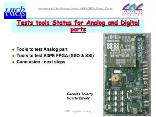
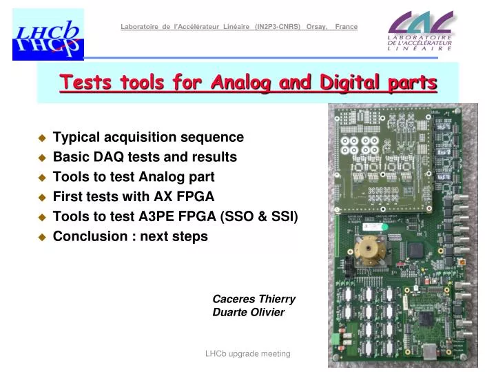
Tests tools for Analog and Digital parts. Typical acquisition sequence Basic DAQ tests and results Tools to test Analog part First tests with AX FPGA Tools to test A3PE FPGA (SSO & SSI) Conclusion : next steps. Caceres Thierry Duarte Olivier. Reminder : Typical acquisition sequence.

E N D
Tests tools for Analog and Digital parts Typical acquisition sequence Basic DAQ tests and results Tools to test Analog part First tests with AX FPGA Tools to test A3PE FPGA (SSO & SSI) Conclusion : next steps Caceres Thierry Duarte Olivier LHCb upgrade meeting
Reminder : Typical acquisition sequence Beginning L0 sequence WriteAcq Register (PC) 1 2 3 Time 1 3 2 Trigger Generator 1 2 3 Data readout by USB Write Data Ctrl 25 ns to 65,5µs Discret Time Beginning latency delay Recording data in RAM (512 points) FIFO full End of latency delay • PC write start sequence bit of Acquisition (Acq) Register. • Beginning of L0 sequence. • Each trigger pulse involve pulse shape. • At the end of the latency delay recording 512 points of data (Max). • At the end of the record the system write one “end of acquisition”bit in the Acq_Register. • The PC scrutinize the Acq_Register, when the “end of acquisition” is high the PC download data with the USB interface. LHCb upgrade meeting
Reminder : Basic DAQ tests Discret Time Soft Trigger (or external) Trigger generator block Latency Trigger Generator Trig Pulses Generator Wr FIFO LatencyWr FIFO All times adjustable ADC_7 [11] From Counters Fixed value (Firmware) ADC_5 (12 bits) ADC_1 (12 bits) ADC_7 (12 bits) ADC_3 (12 bits) ADC_4 (12 bits) ADC_0 (12 bits) ADC_6 (12 bits) ADC_2 (12 bits) A3PE SpyFIFO (8 ADC channels) Wr (96x512) Clk 40 Mhz • Fixed data, counter and pulse stand in for ADC data fromanalog mezzanine USB Interface LHCb upgrade meeting
Tools to test Analog part ADC emulation SPY data • FIFO pattern • Generate digital signals • Check FPGA computations • SPY FIFO • storage of processing results • ANALOG PULSE FIFO • generate trigger of analog pulses 96 • PATTERN_FIFO 96 96 8 USB_data Buffer_FIFOs (12x8) USB wr WR RD (96 x 512) {Add 0x1C} 96 1 96 • Wr : USB • Rd : USB or 40 Mhz 96 96 8 1 (x8) 96 USB data 96 0 WR RD • 12 bit ADC data fromAnalog Mezzanine (96 x 512) 8 x 12bits {Add 0x06} setup_ register[9] • SPY_FIFO 0 USB_data • Wr : USB or 40 Mhz • Rd : USB setup_ register[8] 8 8 8 • ANALOG_PULSE_FIFO 8 • Analog Pulse • ( 1 per ADC Channels) ClkUSB WR RD 8 1 USB_data (8 x 512) {Add 0x1F} • Wr : USB • Rd : USB or 40 Mhz Clk 40 Mhz 0 A3PE setup_register[9] Trigger for Analog LHCb upgrade meeting
First tests with AX FPGA • Idea : RAM pattern to test the A3PE IOs functioning by exchanging data between the 2 FPGA (SSO and SSI) A3PE FPGA AX FPGA Rd/Wr Register 32 Bank 0 Bank 0 A3PE A3PE_Clk VccIOB_Var AX_Clk ?? Bank 1 Bank 1 32 Rd/Wr Register VccIOB_Var A3PE_Clk AX_Clk USB interface 1,5v < VccIOB_Var < +2,5v) A3PE_Clk AX A3PE_Clk Delay Chip AX_Clk • Reminder : • ProASIC3 families are based on nonvolatile flash technology • => reprogrammable • The latest antifuse FPGA family • => Not reprogrammable I2C D D D D D D Q Q Q Q Q Q Clk Clk Clk Clk Clk Clk LHCb upgrade meeting
Tools to test A3PE FPGA (SSO & SSI) • Idea : RAM pattern to test the A3PE IOs functioning by exchanging data between the 2 FPGA (SSO and SSI) • USB Rd / Wr the FIFO (To_AX and From_AX). Buffer_FIFOs 32 ClkUSB 1 32 • Sequence: • To_AX _FIFO Rd/Wr by USB • Start commande • Loop on to AX_FIFO until stop command • Programmable latency to capture data from To_AX_FIFOto FROM_AX_FIFO • To_AX_FIFO CLK_1 Rd Wr 0 From Delay Chip (32 x 512) {Add 0x1D} • Wr : USB • Rd : USB or Clk_1 setup_register[11] 8 USB_data 32 32 32 32 32 32 32 • Ctrl. • Wr / Rd • pattern RegUSB 32 BUSMSB AXTOA3PE 32 _q _q1 setup_register[10] 32 • Start / Stop and latency missing (not implemented yet) 32 1 8 • From_AX_FIFO 32 USB_data 32 32 Wr Rd 32 0 (32x 512) 32 32 {Add 0x1E} 32 setup_register[11] • Wr : USB or Clk_1 • Rd : USB BUSLSB AXTOA3PE 8 32 USB_data AX500 A3PE _q3 _q2 LHCb upgrade meeting
Conclusion • Digital electronic is ok, several adjustment have been done (Tests with Carlos at LAL in November). • Do you have other needs of firmware to test the analog mezzanine ? ? • Started Production of third mother digital board (ready in Jannuary) • Should we considered a 8 channel prototype FEB for the end of 2012 with GBT? • Packing is in stand by. Waiting for decision on GBT bandwith. LHCb upgrade meeting
SPARE LHCb upgrade meeting
Reminder : Basic DAQ tests results Fixed value 456 h (1110) Fixed value ABC h (2748) Fixed value ABC h (2748) Fixed value 456 h (1110) Not connected FFF h ? Counters 4095 Channel 8[11] Not connected FFF h ? 2047 Trigger generator block LHCb upgrade meeting
First tests with AX FPGA AX FPGA 32 Bank 0 VccIOB_Var AX_Clk Bank 1 32 VccIOB_Var AX_Clk 1,5v < VccIOB_Var < +2,5v) • Reminder : • ProASIC3 families are based on not volatile flash technology • => reprogrammable • AX is the latest antifuse FPGA family • => Not reprogrammable • AX programmation with Silicon Scultor D D Q Q Clk Clk LHCb upgrade meeting
Clock tree LHCb upgrade meeting