Download
1 / 27
1k likes | 2.13k Views
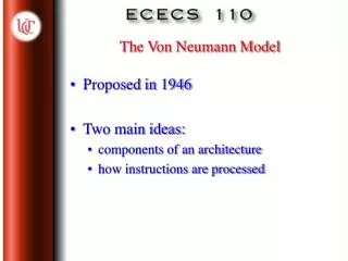
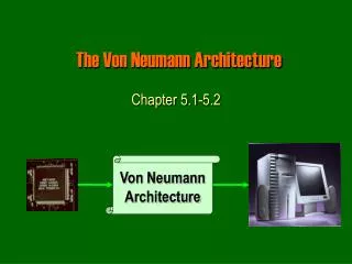
The Von Neumann Architecture. Chapter 5.1-5.2. Von Neumann Architecture. Designing Computers. All computers more or less based on the same basic design, the Von Neumann Architecture !. The Von Neumann Architecture.

E N D
The Von Neumann Architecture Chapter 5.1-5.2 Von Neumann Architecture
Designing Computers • All computers more or less based on the same basic design, the Von Neumann Architecture! (c) Yngvi Bjornsson
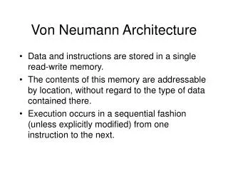
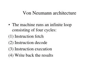
The Von Neumann Architecture • Model for designing and building computers, based on the following three characteristics: • The computer consists of four main sub-systems: • Memory • ALU (Arithmetic/Logic Unit) • Control Unit • Input/Output System (I/O) • Program is stored in memory during execution. • Program instructions are executed sequentially. (c) Yngvi Bjornsson
Communicate with • "outside world", e.g. • Screen • Keyboard • Storage devices • ... Store data and program Execute program Do arithmetic/logic operationsrequested by program The Von Neumann Architecture Bus Memory Processor (CPU) Input-Output Control Unit ALU (c) Yngvi Bjornsson
Memory Subsystem • Memory, also called RAM (Random Access Memory), • Consists of many memory cells (storage units) of a fixed size. Each cell has an address associated with it: 0, 1, … • All accesses to memory are to a specified address.A cell is the minimum unit of access (fetch/store a complete cell). • The time it takes to fetch/store a cell is the same for all cells. • When the computer is running, both • Program • Data (variables) are stored in the memory. (c) Yngvi Bjornsson
RAM N 0000000000000001 • Need to distinguish between • the address of a memory cell and the content of a memory cell • Memory width (W): • How many bits is each memory cell, typically one byte (=8 bits) • Address width (N): • How many bits used to represent each address, determines the maximum memory size = address space • If address width is N-bits, then address space is 2N (0,1,...,2N-1) 1 bit 0 1 2 ... 2N 2N-1 W (c) Yngvi Bjornsson
Memory Size / Speed • Typical memory in a personal computer (PC): • 64MB - 256MB • Memory sizes: • Kilobyte (KB) = 210 = 1,024 bytes ~ 1 thousand • Megabyte(MB) = 220 = 1,048,576 bytes ~ 1 million • Gigabyte (GB) = 230 = 1,073,741,824 bytes ~ 1 billion • Memory Access Time (read from/ write to memory) • 50-75 nanoseconds (1 nsec. = 0.000000001 sec.) • RAM is • volatile (can only store when power is on) • relatively expensive (c) Yngvi Bjornsson
Operations on Memory • Fetch (address): • Fetch a copy of the content of memory cell with the specified address. • Non-destructive, copies value in memory cell. • Store (address, value): • Store the specified value into the memory cell specified by address. • Destructive, overwrites the previous value of the memory cell. • The memory system is interfaced via: • Memory Address Register (MAR) • Memory Data Register (MDR) • Fetch/Store signal (c) Yngvi Bjornsson
Structure of the Memory Subsystem • Fetch(address) • Load address into MAR. • Decode the address in MAR. • Copy the content of memory cell with specified address into MDR. • Store(address, value) • Load the address into MAR. • Load the value into MDR. • Decode the address in MAR • Copy the content of MDR into memory cell with the specified address. MAR MDR F/S Memory decoder circuit Fetch/Store controller ... (c) Yngvi Bjornsson
Input/Output Subsystem • Handles devices that allow the computer system to: • Communicate and interact with the outside world • Screen, keyboard, printer, ... • Store information (mass-storage) • Hard-drives, floppies, CD, tapes, … • Mass-Storage Device Access Methods: • Direct Access Storage Devices (DASDs) • Hard-drives, floppy-disks, CD-ROMs, ... • Sequential Access Storage Devices (SASDs) • Tapes (for example, used as backup devices) (c) Yngvi Bjornsson
I/O Controllers • Speed of I/O devices is slow compared to RAM • RAM ~ 50 nsec. • Hard-Drive ~ 10msec. = (10,000,000 nsec) • Solution: • I/O Controller, a special purpose processor: • Has a small memory buffer, and a control logic to control I/O device (e.g. move disk arm). • Sends an interrupt signal to CPU when done read/write. • Data transferred between RAM and memory buffer. • Processor free to do something else while I/O controller reads/writes data from/to device into I/O buffer. (c) Yngvi Bjornsson
Structure of the I/O Subsystem Interrupt signal (to processor) Data from/to memory I/O controller I/O Buffer Control/Logic I/O device (c) Yngvi Bjornsson
The ALU Subsystem • The ALU (Arithmetic/Logic Unit) performs • mathematical operations (+, -, x, /, …) • logic operations (=, <, >, and, or, not, ...) • In today's computers integrated into the CPU • Consists of: • Circuits to do the arithmetic/logic operations. • Registers (fast storage units) to store intermediate computational results. • Bus that connects the two. (c) Yngvi Bjornsson
GT EQ LT Structure of the ALU R0 • Registers: • Very fast local memory cells, that store operands of operations and intermediate results. • CCR (condition code register), a special purpose register that stores the result of <, = , > operations • ALU circuitry: • Contains an array of circuits to do mathematical/logic operations. • Bus: • Data path interconnecting the registers to the ALU circuitry. R1 R2 Rn ALU circuitry (c) Yngvi Bjornsson
The Control Unit • Program is stored in memory • as machine language instructions, in binary • The task of the control unit is to execute programs by repeatedly: • Fetch from memory the next instruction to be executed. • Decode it, that is, determine what is to be done. • Execute it by issuing the appropriate signals to the ALU, memory, and I/O subsystems. • Continues until the HALT instruction (c) Yngvi Bjornsson
Machine Language Instructions • A machine language instruction consists of: • Operation code, telling which operation to perform • Address field(s), telling the memory addresses of the values on which the operation works. • Example: ADD X, Y (Add content of memory locations X and Y, and store back in memory location Y). • Assume: opcode for ADD is 9, and addresses X=99, Y=100 Opcode (8 bits) Address 1 (16 bits) Address 2 (16 bits) 00001001 0000000001100011 0000000001100100 (c) Yngvi Bjornsson
Instruction Set Design • Two different approaches: • Reduced Instruction Set Computers (RISC) • Instruction set as small and simple as possible. • Minimizes amount of circuitry --> faster computers • Complex Instruction Set Computers (CISC) • More instructions, many very complex • Each instruction can do more work, but require more circuitry. (c) Yngvi Bjornsson
Typical Machine Instructions • Notation: • We use X, Y, Z to denote RAM cells • Assume only one register R (for simplicity) • Use English-like descriptions (should be binary) • Data Transfer Instructions • LOAD X Load content of memory location X to R • STORE X Load content of R to memory location X • MOVE X, Y Copy content of memory location X to loc. Y (not absolutely necessary) (c) Yngvi Bjornsson
Machine Instructions (cont.) • Arithmetic • ADD X, Y, Z CON(Z) = CON(X) + CON(Y) • ADD X, Y CON(Y) = CON(X) + CON(Y) • ADD X R = CON(X) + R • similar instructions for other operators, e.g. SUBTR,OR, ... • Compare • COMPARE X, YCompare the content of memory cell X to the content of memory cell Y and set the condition codes (CCR) accordingly. • E.g. If CON(X) = R then set EQ=1, GT=0, LT=0 (c) Yngvi Bjornsson
Machine Instructions (cont.) • Branch • JUMP X Load next instruction from memory loc. X • JUMPGT X Load next instruction from memory loc. X only if GT flag in CCR is set, otherwise load statement from next sequence loc. as usual. • JUMPEQ, JUMPLT, JUMPGE, JUMPLE,JUMPNEQ • Control • HALT Stop program execution. (c) Yngvi Bjornsson
Example • Pseudo-code: Set A to B + C • Assuming variable: • A stored in memory cell 100, B stored in memory cell 150, C stored in memory cell 151 • Machine language (really in binary) • LOAD 150 • ADD 151 • STORE 100 • or • (ADD 150, 151, 100) (c) Yngvi Bjornsson
Structure of the Control Unit • PC (Program Counter): • stores the address of next instruction to fetch • IR (Instruction Register): • stores the instruction fetched from memory • Instruction Decoder: • Decodes instruction and activates necessary circuitry PC IR +1 Instruction Decoder (c) Yngvi Bjornsson
von Neumann Architecture (c) Yngvi Bjornsson
How does this all work together? • Program Execution: • PC is set to the address where the first program instruction is stored in memory. • Repeat until HALT instruction or fatal error Fetch instruction Decode instruction Execute instruction End of loop (c) Yngvi Bjornsson
Program Execution (cont.) • Fetch phase • PC --> MAR (put address in PC into MAR) • Fetch signal (signal memory to fetch value into MDR) • MDR --> IR (move value to Instruction Register) • PC + 1 --> PC (Increase address in program counter) • Decode Phase • IR -> Instruction decoder (decode instruction in IR) • Instruction decoder will then generate the signals to activate the circuitry to carry out the instruction (c) Yngvi Bjornsson
Program Execution (cont.) • Execute Phase • Differs from one instruction to the next. • Example: • LOAD X (load value in addr. X into register) • IR_address -> MAR • Fetch signal • MDR --> R • ADD X • left as an exercise (c) Yngvi Bjornsson
Instruction Set for Our Von Neumann Machine (c) Yngvi Bjornsson