Download
1 / 85
920 likes | 1.55k Views
Chapter 5 Differential and Multistage Amplifier. Outline. Introduction The CMOS Differential Pair Small-Signal Operation of the MOS Differential Pair The BJT Differential Pair The differential Amplifier with Active Load Frequency Response of the Differential amplifier

E N D
Chapter 5Differential and Multistage Amplifier SJTU Zhou Lingling
Outline • Introduction • The CMOS Differential Pair • Small-Signal Operation of the MOS Differential Pair • The BJT Differential Pair • The differential Amplifier with Active Load • Frequency Response of the Differential amplifier • Multistage Amplifiers SJTU Zhou Lingling
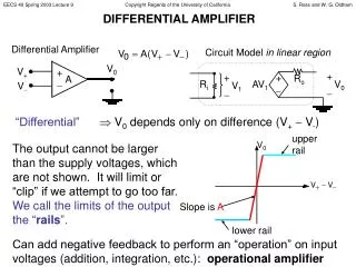
Introduction • Two reasons of the differential amplifier suited for IC fabrication: • IC fabrication is capable of providing matched devices. • Utilizing more components than single-ended amplifier: • Differential circuits are much less sensitive to noise and interference. • Differential configuration enable us to bias the amplifier and to couple amplifier stages without the need for bypass and coupling capacitors. SJTU Zhou Lingling
The MOS Differential Pair • Basic structure of differential pair. • Characteristics SJTU Zhou Lingling
The MOS Differential Pair SJTU Zhou Lingling
Operation with a Common –Mode Input Voltage SJTU Zhou Lingling
Operation with a Common –Mode Input Voltage • Symmetry circuit. • Common-mode voltage. • Current I divides equally between two transistors. • The difference between two drains is zero. • The differential pair rejects the common-mode input signals. SJTU Zhou Lingling
Operation with a Differential Input Voltage • The MOS differential pair with a differential input signal vid applied. • With vid positive: vGS1>vGS2, iD1>iD2, and vD1<vD2; thus (vD2-vD1) will be positive. • With vid negative: vGS1<vGS2, iD1<iD2, and vD1>vD2; thus (vD2-vD1) will be negative. SJTU Zhou Lingling
Operation with a Differential Input Voltage • Differential input voltage. • Response to the differential input signal. • The current I can be steered from one transistor to the other by varying the differential input voltage in the range: • When differential input voltage is very small, the differential output voltage is proportional to it, and the gain is high. SJTU Zhou Lingling
Large-Signal Operation • Transfer characteristic curves • Normalized plots of the currents in a MOSFET differential pair. • Note that VOV is the overdrive voltage at which Q1 and Q2 operate when conducting drain currents equal to I/2. SJTU Zhou Lingling
Large-Signal Operation • Nonlinear curves. • Maximum value of input differential voltage. • When vid= 0, two drain currents are equal to I/2. • Linear segment. • Linearity can be increased by increasing overdrive voltage(see next slide). • Price paid is a reduction in gain(current I is kept constant). SJTU Zhou Lingling
Large-Signal Operation The linear range of operation of the MOS differential pair can be extended by operating the transistor at a higher value of VOV. SJTU Zhou Lingling
Small-Signal Operation of MOS Differential Pair • Linear amplifier • Differential gain • Common-mode gain • Common-mode rejection ratio(CMRR) • Mismatch on CMRR SJTU Zhou Lingling
Differential Gain • a common-mode voltage applied to set the dc bias voltage at the gates. • vid applied in a complementary (or balanced) manner. SJTU Zhou Lingling
Differential Gain Signal voltage at the joint source connection must be zero. SJTU Zhou Lingling
Differential Gain An alternative way of looking at the small-signal operation of the circuit. SJTU Zhou Lingling
Differential Gain • Differential gain • Output taken single-ended • Output taken differentially • Advantages of output signal taken differentially • Reject common-mode signal • Increase in gain by a factor of 2(6dB) SJTU Zhou Lingling
Differential Gain MOS differential amplifier with ro and RSS taken into account. SJTU Zhou Lingling
Differential Gain • Equivalent circuit for determining the differential gain. • Each of the two halves of the differential amplifier circuit is a common-source amplifier, known as its differential “half-circuit.” SJTU Zhou Lingling
Differential Gain • Differential gain • Output taken single-ended • Output taken differentially SJTU Zhou Lingling
Common-Mode Gain The MOS differential amplifier with a common-mode input signal vicm. SJTU Zhou Lingling
Common-Mode Gain • Equivalent circuit for determining the common-mode gain (with ro ignored). • Each half of the circuit is known as the “common-mode half-circuit.” SJTU Zhou Lingling
Common-Mode Gain • Common-mode gain • Output taken single-ended • Output taken differentially SJTU Zhou Lingling
Common-Mode Rejection Ratio • Common-mode rejection ratio(CMRR) • Output taken single-ended • Output taken differentially This is true only when the circuit is perfectly matched. SJTU Zhou Lingling
Mismatch on CMRR • Effect of RD mismatch on CMRR • Effect of gm mismatch on CMRR SJTU Zhou Lingling
Mismatch on CMRR • Determine the common-mode gain resulting from a mismatch in the gm values of Q1 and Q2. • Common-mode half circuit is not available due to mismatch in circuit. • The nominal value gm. SJTU Zhou Lingling
Mismatch on CMRR • Effect of gm mismatch on CMRR SJTU Zhou Lingling
The BJT Differential Pair • Basic operation • Large-signal operation • Small-signal operation • Differential gain • Common-mode gain • Common-mode rejection ration SJTU Zhou Lingling
The BJT Differential Pair The basic BJT differential-pair configuration. SJTU Zhou Lingling
Basic Operation • The differential pair with a common-mode input signal vCM. • Two transistors are matched. • Current source with infinite output resistance. • Current I divide equally between two transistors. • The difference in voltage between the two collector is zero. • The differential pair rejects the common-mode input signal as long as two transistors remain in active region. SJTU Zhou Lingling
Basic Operation • The differential pair with a “large” differential input signal. • Q1 is on and Q2 is off. • Current I entirely flows in Q1. SJTU Zhou Lingling
Basic Operation • The differential pair with a large differential input signal of polarity opposite to that in (b). • Q2 is on and Q1 is off. • Current I entirely flows in Q2. SJTU Zhou Lingling
Basic Operation • The differential pair with a small differential input signal vi. • Small signal operation or linear amplifier. • Assuming the bias current source I to be ideal and thus I remains constant with the change in vCM. • Increment in Q1 and decrement in Q2. SJTU Zhou Lingling
Large-Signal Operation SJTU Zhou Lingling
Large-Signal Operation • Nonlinear curves. • Linear segments. • Maximum value of input differential voltages • Enlarge the linear segment by including equal resistance Re in series with the emitters. SJTU Zhou Lingling
Large-Signal Operation The transfer characteristics of the BJT differential pair (a) can be linearized by including resistances in the emitters. SJTU Zhou Lingling
Small Signal Operation The currents and voltages in the differential amplifier when a small differential input signal vid is applied. SJTU Zhou Lingling
Small Signal Operation A simple technique for determining the signal currents in a differential amplifier excited by a differential voltage signal vid; dc quantities are not shown. SJTU Zhou Lingling
Small Signal Operation • A differential amplifier with emitter resistances. • Only signal quantities are shown (in color). SJTU Zhou Lingling
Input Differential Resistance • Input differential resistance is finite. The resistance seen between the two bases is equal to the total resistance in the emitter circuit multiplied by (1+β). • Input differential resistance of differential pair with emitter resistors. SJTU Zhou Lingling
Differential Voltage Gain • Differential voltage gain • Output voltage taken single-ended • Output voltage taken differentially SJTU Zhou Lingling
Differential Voltage Gain • Differential voltage gain of the differential pair with resistances in the emitter leads • Output voltage taken single-ended • Output voltage taken differentially The voltage gain is equal to the ratio of the total resistance in the collector circuit to the total resistance in the emitter circuit. SJTU Zhou Lingling
Differential Half-Circuit Analysis • Differential input signals. • Single voltage at joint emitters is zero. • The circuit is symmetric. • Equivalent common-emitter amplifiers in (b). SJTU Zhou Lingling
Differential Half-Circuit Analysis • This equivalence applies only for differential input signals. • Either of the two common-emitter amplifiers can be used to find the differential gain, differential input resistance, frequency response, and so on, of the differential amplifier. • Half circuit is biased at I/2. • The voltage gain(with the output taken differentially) is equal to the voltage of half circuit. SJTU Zhou Lingling
Differential Half-Circuit Analysis • The differential amplifier fed in a single-ended fashion. • Signal voltage at the emitter is not zero. • Almost identical to the symmetric one. SJTU Zhou Lingling
Common-Mode Gain The differential amplifier fed by a common-mode voltage signal vicm. SJTU Zhou Lingling
Common-Mode Gain Equivalent “half-circuits” for common-mode calculations. SJTU Zhou Lingling
Common-Mode Gain • Common-mode voltage gain • Output voltage taken single-ended • Output voltage taken differentially SJTU Zhou Lingling
Common-Mode Rejection Ratio • Common-mode rejection ratio • Output voltage taken single-ended • Output voltage taken differentially This is true only when the circuit is symmetric. • Mismatch on CMRR SJTU Zhou Lingling
Input Common-Mode Resistance • Definition of the input common-mode resistance Ricm. • The equivalent common-mode half-circuit. SJTU Zhou Lingling