Advanced X-ray Microscopy for Studying Bulk Materials
20 likes | 124 Views
Explore how new X-ray microscopy technology characterizes thousands of crystals within bulk materials, tracking structural changes during processing. This innovative method provides valuable experimental data for computational materials models, contributing to the understanding of material behavior and degradation. Supported by NSF funding, graduate students play a key role in advancing this technique, attracting interest from collaborators and industry experts worldwide.

Advanced X-ray Microscopy for Studying Bulk Materials
E N D
Presentation Transcript
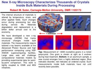
New X-ray Microscopy Characterizes Thousands of Crystals Inside Bulk Materials During Processing Robert M. Suter, Carnegie-Mellon University, DMR 1105173 The internal structure of materials is altered by temperature, strain, and other applied fields. Such changes occur during processing but also during service life. Materials degradation and replacement is a billion dollar annual cost to the economy. We have developed a new x-ray microscopy (HEDM) that tracks structural changes inside bulk materials. The measurements require tailored x-ray beams available at the Advanced Photon Source and high performance computing using NSF XSEDE supercomputing facilities. Large data sets will challenge computational materials models by providing experimental data for point-by-point comparison. This work is tightly coupled to ICME and MGI initiatives. 1 millimeter Top: Measurement of ~4000 crystalline grains in a nickel polycrystal. One grain is shown at right as it evolves during heat treatment. Bottom: In an aluminum sample, a new crystal emerges from a highly defected region. Blue indicates disorder, red indicates an ordered crystal. Such measurements inside bulk materials have not until recently been possible.
New X-ray Microscopy Characterizes Thousands of Crystals Inside Bulk Materials During Processing Robert M. Suter, Carnegie-Mellon University, DMR 1105173 • Broader Impact • Supported graduate students are world experts on the experimental and computational aspects of an innovative new technique for studying materials evolution under a variety of stimuli. They are among the first to develop characterization tools for these studies. Students supported by the NSF program are sought by both collaborators and industrial and national laboratory employers. • The facility at the Advanced Photon Source beamline is known worldwide for its leading role in HEDM measurements. Both materials scientists and materials engineers are attracted by the unique capabilities. • The materials modeling community is increasingly looking to HEDM to provide critical datasets to test understanding of materials responses. Graduate students Xit Tan, Jonathan Lind, and Reeju Polkharel in the experiment hutch at the Advanced Photon Source during commissioning of a new imaging detector for HEDM and tomography measurements.
