Download
1 / 2
20 likes | 160 Views
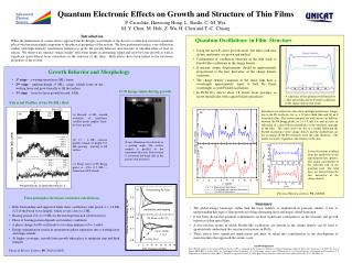
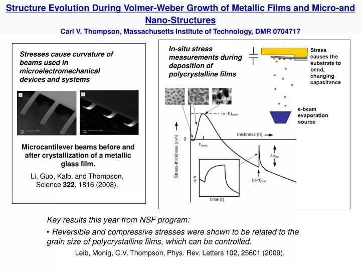
Structure Evolution During Volmer-Weber Growth of Metallic Films and Micro-and Nano-Structures Carl V. Thompson, Massachusetts Institute of Technology, DMR 0704717. In-situ stress measurements during deposition of polycrystalline films.

E N D
Structure Evolution During Volmer-Weber Growth of Metallic Films and Micro-and Nano-Structures Carl V. Thompson, Massachusetts Institute of Technology, DMR 0704717 In-situ stress measurements during deposition of polycrystalline films Stresses cause curvature of beams used in microelectromechanical devices and systems Microcantilever beams before and after crystallization of a metallic glass film. Li, Guo, Kalb, and Thompson, Science 322, 1816 (2008). • Key results this year from NSF program: • Reversible and compressive stresses were shown to be related to the grain size of polycrystalline films, which can be controlled. • Leib, Monig, C.V. Thompson, Phys. Rev. Letters 102, 25601 (2009).
Structure Evolution During Volmer-Weber Growth of Metallic Films and Micro-and Nano-Structures Carl V. Thompson, Massachusetts Institute of Technology, DMR 0704717 Results from NSF research have been included in MIT courses: 3.44 Materials Processing for Micro- and Nano-Systems 3.47 Materials Processing at the Nano-Scale 3.48J* Materials and Processes for Microelectromechanical Devices and Systems and courses for professional engineers and scientists in summer short courses: Industry: Materials Science and Engineering for Integrated Circuits and Microelectromechanical Systems (HP and Chartered Semiconductor). University-based:Introduction to Processing and Properties of Nanoscale Materials (National University of Singapore). * jointly offered in 5 engineering departments at MIT, and simultaneously beamed to Singapore As the Director of MIT’s Materials Processing Center, the PI organizes numerous out-reach activities: 2008 summer interns from other universities (Co-organized with NSF MRSEC program) ‘MIT Materials Day’ student poster ward winners Industry workshop: ‘Nanostructure to Infrastructure’ Stuttgart