Download
1 / 18
240 likes | 427 Views
Carbon Nanotubes for Small Antennas. Janet Werth, Sarah O’Donnell, Lucien Teig, David Lamensdorf, Aleksandra Markina, Jim Marshall MITRE Sponsored Research. Approved for Public Release Distribution Unlimited Case # 09-1881. © 2009 The MITRE Corporation. All rights reserved.

E N D
Carbon Nanotubes for Small Antennas Janet Werth, Sarah O’Donnell, Lucien Teig, David Lamensdorf, Aleksandra Markina, Jim Marshall MITRE Sponsored Research Approved for Public ReleaseDistribution UnlimitedCase # 09-1881 © 2009 The MITRE Corporation. All rights reserved.
Problem Statement and Objectives • Problem • There is a great need for small efficient antennas • Electrically small antennas have significant loss in matching • Wideband antennas are less efficient, do not provide spectral filtering, and antenna coverage varies with frequency • Objective: Exploit the unique properties of CNTs to advance the state-of-the-art in small efficient antennas CNT = Carbon Nanotube 2 © 2009 The MITRE Corporation. All rights reserved.
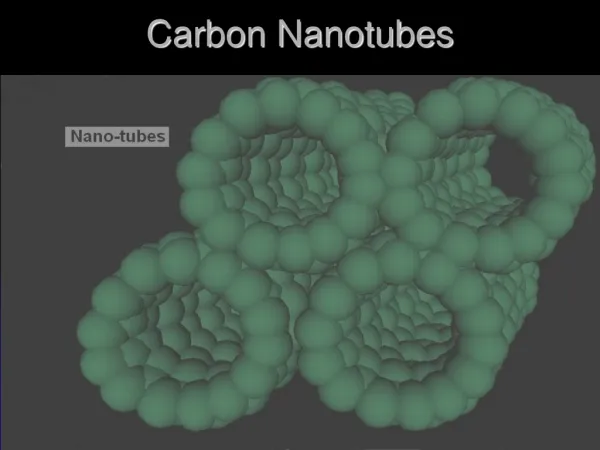
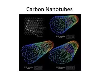
Multiwall CNT What is a Carbon Nanotube? • Single Wall Carbon Nanotube (SWNT) • Graphite sheet seamlessly wrapped to form a cylinder typically 1 nm in diameter • Properties • Higher electrical current density and thermal conductivity than any metals • BALLISTIC ELECTRON TRANSPORT – i.e., no backscattering of electrons,which is the a source of electrical resistance • McEuen (Cornell) measuring conduction vs. length of SWNT show ballistic length limited to ~1.2 microns • Mechanically stronger than most if not all other materials SWNT Bundles 3 R. H. Baughman et al, “Carbon Nanotubes – the Route Toward Applications”, Science, vol. 297, 2 Aug. 2002, p787-792 © 2009 The MITRE Corporation. All rights reserved.
Work Program Exploit the unique properties of CNTs to advance the state of the art in small antenna design FY0 Reconfigurable Antenna Development Efficient Electrically Small Antennas 1 2 Extend Lossless Length of CNTs Photovoltaic CNT based Switch CNT Inductor Electronically Reconfigurable Dual Band Monopole Electrically Short Monopole Theoretical Analysis Hardware Prototype 4 © 2009 The MITRE Corporation. All rights reserved.
ApplicationCNTs for Small Antenna Matching Networks • Concept - minimize resistive loss in tuning networks • Benefit from high conductivity and high current density of CNT • Application – Enable efficient electrically very short antennas • Resistance of regular inductor is much higher than antenna radiation resistance • Smaller batteries required for sensors or longer battery life • Challenges • Ballistic transport length • Current density inversely proportional to CNT length • Connection to RF circuitry • Bundling and associated behavior 5 © 2009 The MITRE Corporation. All rights reserved.
Functionalization to Enhance Conduction Property of CNT’s Bonding along individual or bundle of CNT • Objective: • Increase (>1.2 um) ballistic (lossless) transport length for SWCNTs • Chemically bond ligands to specific locations on sidewalls of CNT to modify low energy phonon spectrum • Analyze applicability to proposed RF applications (e.g., bending for toroid, helical inductor) • First Principles Quantum Mechanics – Professor Marzari of MIT • Efficient calculation of CNT band/ligand structure Courtesy of Prof. Marzari of MIT 6 © 2009 The MITRE Corporation. All rights reserved.
Application - Reconfigurable Apertures • Electronically tune antenna in “real time” using switches • Multiple band operation using one antenna • Minimize footprint and physical connections to platform • Nanoswitch attributes • Optical activation – no wire to control switch • Overcomes size, and power consumption challenges with existing FET and MEMs switches. Similar to MEMs switch, but smaller • High reliability (no moving parts) • Low loss (negligible power consumption) • Resistant to extreme temperature variations, magnetism Lockheed Sanders Georgia Tech Research Institute 7 © 2009 The MITRE Corporation. All rights reserved.
Motivation - Reconfigurable Apertures • Platform Challenge • Limited Real Estate • Aerodynamic drag • Installation costs are high • Concept • Single electronically tunable aperture • Frequency • Polarization • Spectrum management over wideband antenna Tunable Monopole Example 25 cm Z 18.8 cm 18.7 cm Low Band High Band Switchable dual band monopole Enabling Technology is CNT-Based Optically Activated Switch 8 © 2009 The MITRE Corporation. All rights reserved.
13 cm 2 mm 16.8 cm 3.5 cm diameter Switch Design Methodology/Accomplishment • Switch design (Complete) • CNT parameters (density, length, contacts, metallic vs. semiconducting, ..) • Photovoltaic COTS designs • Prototype development (In process) • Based on Univ. of Illinois (Prof. Rogers) developed CNT growth technology with minor modifications • Equivalent circuit (lumped circuit elements for antenna studies) • Antenna analysis • Monopole with ideal gap (complete) • Monopole with equivalent circuit across gap • Monopole integration and test at 250 and 400 MHz design frequencies 9 © 2009 The MITRE Corporation. All rights reserved.
Whole (“connected”) and cut tube monopole antennas were simulated using the MoM code Patch Finite ground plane Connected antenna approximates a configuration with a closed switch (250 MHz) Cut antenna approximates a configuration with an open switch (400 MHz) Simulate antenna performance with circuit model 13 cm 2 mm 3.5 cm diameter 16.8 cm 3.5 cm diameter Antenna Analysis: Sample Monopole Antenna 30 cm 3.5 cm diameter Ground Plane 10 © 2009 The MITRE Corporation. All rights reserved.
Antenna Analysis:Monopole on Circular Ground Plane 250 MHz 400 MHz Uncut • Impedance = 199.08 Ohm • Mismatch = -2.58 dB • VSWR = 5.05 • Impedance = 48.48 Ohm • Mismatch = -0.08 dB • VSWR = 1.31 Cut • Impedance = 51.55 Ohm • Mismatch = -0.01 dB • VSWR = 1.11 • Impedance = 65.54 Ohm • Mismatch = -5.64 dB • VSWR = 12.59 Tuned antenna patterns between and 30 and 90 degrees Provide nearly the same gain when the antenna is tuned 11 © 2009 The MITRE Corporation. All rights reserved.
COTS Solar Cell Drain Gate Source Solar Cell Switch Design: U of Illinois FET Measured in MITRE Lab Drain Aligned CNTs Source Gate 12 ~1 mm © 2009 The MITRE Corporation. All rights reserved.
Electrical Resistance Elements • R= h/4e2+Ri+Rc1+Rc2 • Ri is intrinsic differential resistance caused by phonon scattering, lattice impurities in CNT • Rc is contact resistance caused by transport barrier at CNT- electrode junction • Rc =h/(4e2T) where T ≤ 1 is the transmission probability across the junction • h/4e2 is ohmic loss due to conservation of energy • McEuen experiments use contacts and measure conductance versus length 13 © 2009 The MITRE Corporation. All rights reserved.
Switch Design:Parasitic Coupling Analysis Source to Drain capacitance calculations using FastCap Drain Gate Source • Vertical dimension of conductors greatly exaggerated (~100 times) • In this version, gap is 2 x 5 microns and 1 micron wide gate is present Trade space: CNT density, CNT length, capacitance and loss. CNT resistance increases with gate and gap width. Resistance decreases with increasing CNT density. 14 © 2009 The MITRE Corporation. All rights reserved.
10M 1M 100k 10k 1k CNT length (m) Switch Design:Impact of Contact and CNT Resistance • For 100k contact R, we double R at ~10 µm • For 30k contact R, we double R at ~ 3 µm • For 10k contact R, we double R at ~ 1 µm CNT Resistance (contact + tubes) • Design: • Minimize contact resistance and maximize nanotubes density • Device Resistance (at 0 CNT length) with 5 CNTs per µ on two gaps of 600 µ length • 16 for 100k contact resistance • 5 for 30k contact resistance The final switch parameters will be determined as CNT processes evolve to meet our design specifications 15 © 2009 The MITRE Corporation. All rights reserved.
Switch Design and Prototype Methodology • University of Illinois CNT growth technology based upon our design layout • Minimize contact resistance • Maximize nanotube density • Eliminate metallic tubes 16 © 2009 The MITRE Corporation. All rights reserved.
Switch Design – Work Remaining Losses that can be theoretically overcome with electronically tunable design • Complete Device Demonstration Steps with final device • Steps have been demonstrated with interim unit • RF measurements with final device • Develop circuit model for our switch design • Insert circuit model into antenna model to obtain antenna pattern and efficiency Example of Equivalent Circuit Model 17 © 2009 The MITRE Corporation. All rights reserved.
Impact • Antennas • Build the foundation for efficient electrically small antennas • Enable reconfigurable apertures suitable multi-function applications • Mechanical structures • Computational techniques extensible • CNT based application maturity • Knowledge base will allow future application of CNTs as electrical elements for JTRS, FAB-T, MP-CDL, ESAs, etc. • Self healing fiber resin composite • Apply CNT expertise to address other CNT applications such as biosensors given their sensitivity to gases and oxygen Enables new classes of antennas Electrically small antennas and reconfigurable apertures Functionalization will extend use of CNT ballistic transport behavior 18 © 2009 The MITRE Corporation. All rights reserved.