Download
1 / 50
1.35k likes | 2.42k Views
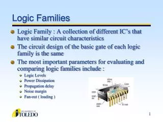
LOGIC FAMILIES. By: Dr. Hetal Patel. Digital Logic Families. Three commonly used families: TTL (transistor-transistor logic) CMOS (complementary metal oxide semiconductor) ECL (emitter-coupled logic) Subfamilies within each family

E N D
LOGIC FAMILIES By: Dr. Hetal Patel
Digital Logic Families • Three commonly used families: • TTL (transistor-transistor logic) • CMOS (complementary metal oxide semiconductor) • ECL (emitter-coupled logic) • Subfamilies within each family • Different speed, power consumption, voltage and current levels, and temperature ranges • There are standardized numbering schemes but prefixes may differ
The TTL Family • NPN bipolar transistor • Physical model • Schematic symbol • Diode equivalent 4
The TTL Family • Two-input NAND gate • Multi-emitter transistor • Totem-pole output stage • HIGH level output typically 3.4 V • LOW level output typically 0.3 V 5
The TTL Family • 7400 two-input NAND gate 6
TTL Voltage and Current Ratings • Input/output current • Source current – IOH • Sink current – IOL • Low-level input current – IIL • High level input current – IIH 7
TTL Voltage and Current Ratings • Fan-out is the number of gate inputs of the same sub-family that a single output can drive. • The IOH rating must be greater-than or equal-to the sum of all IHS ratings. 7
TTL Voltage and Current Ratings • Example of TTL gate sinking input currents from two gate inputs using logic symbols 8
TTL Voltage and Current Ratings • Example of TTL gate sinking input currents from two gate inputs using schematic symbols 9
TTL Voltage and Current Ratings • Example of TTL gate sourcing current to two gate inputs using logic symbols 10
TTL Voltage and Current Ratings • Example of TTL gate sourcing current to two gate inputs using schematic symbols 11
TTL Voltage and Current Ratings • Summary of I/O current and fan-out: • Low-level input current IIL = -1.6 mA (-1600 μA) • High level input current IIH= 40 μA • (The minus sign indicates current leaving the gate) • IOL– low-level output current = 16 mA (16,000 μA) • IOH – high-level output current = -400 μA (-800 μA for some) • Fan-out is max number of gate inputs that can be connected to a standard TTL gate output. • Typically fan-out = 10. • Note: Current ratings are not the amount of current, but the maximum current capability. 12
TTL Voltage and Current Ratings • Input/Output Voltages (graphical representation) 14
Noise Margin • Noise margin: The difference between high level voltages and low level voltages 13
TTL Voltage and Current Ratings • Input/Output Voltages and noise margin 14
Pulse-Time Parameters • Rise Time (tr) – Measured from 10% level to 90% level • Fall Time (tf) – Measured from 90% level to 10% level 20
Propagation Delay • Propagation Delay (tPLH and tPHL) • Determined by transistor switching speed 22
Power Dissipation • Total power supplied to the IC power supply terminals • Assume 50% duty cycle. • PD = VCC x ICC(av) 23
Open-Collector Outputs • Upper transistor is removed • Can sink current but cannot source current
Open-Collector Outputs • To get a TTL OC output or a CMOS OD output to produce a HIGH, a pull-up resistor is required.
Wired-output operation • Outputs from two or more gates tied together • Wired-AND logic 24
Other TTL Considerations • Power supply decoupling • TTL logic tends to produce spikes on the VCC line • Connecting a 0.01 to 0.1 F capacitor between VCC and ground pins • Reduces EMI radiation • Reduces effect of voltage spikes from power supply • Should installed close to the IC 26
Improved TTL Series • 74HXX series • Half the propagation delay • Double the power consumption • 74LXX series • Twice the propagation delay • Half the power consumption • In both cases the speed-power product remained about the same. • In most cases both have been replaced by Schottky TTL and CMOS. 27
Schottky TTL • Main speed limitation of standard TTL is due to capacitive charge in transistor base. • Charge is stored when saturated • 74SXX TTL series adds a Schottky diode between the base and collector. 27
Schottky TTL • Lower-power Schottky (LS) • Power consumption significantly reduced • Speed-power product 1/3 of 74SXX series and 1/5 of 74XX series • Advanced low-power Schottky (ALS) • Propagation delay dropped from 9 to 4 ns • Power dissipation from 2 to 1 mW per gate • More expensive • Fast (F) • Propagation lowered to under 3 ns. • Device size dramatically reduced 27
The CMOS Family • MOSFETs • Metal oxide semiconductor field-effect transistors • High input impedance and low power dissipation 28
Gate-to-source voltage VGSis the input voltage. • Used to control resistance between drain & source. • Determines whether the device is on or off.
The CMOS Family • N-Channel MOSFET • Built on P material • Normally OFF • Positive gate voltage induces the N-channel • P-channel MOSFET • Channel is formed by a positive gate voltage • Three major MOS families • PMOS: P-channel • NMOS: N-channel • CMOS: Complimentary P- and N-channel 30
P-MOS & N-MOS circuits began to dominate the LSI and VLSI markets in the 1970s and 1980s. • Use fewer components & are much simpler to manufacture than TTL circuits. • During this era, technology emerged that usedP-MOS & N-MOS transistors in the same circuit. • Complementary MOS, or CMOS, technology.
The CMOS Family • CMOS inverter formed from N-and P-channel MOSFETS. 30
Handling CMOS devices • Avoid electrostatic discharge • Ground work station, test equipment and soldering irons • Wear a wrist strap • Don’t connect input signals with power off • Connected unused inputs to VDD • Don’t remove IC with power on 30
CMOS IC Series • The oldest CMOS series is the 4000 series by RCA—functionally equivalent to Motorola 14000. • Rarely used in new designs except when a special-purpose IC is not available in other series. • The 74HC/HCT series has a 10-fold increase in switching speed, comparable to 74LS devices. • Pin-compatible with, functionally equivalent to TTLICs with the same device number. • The 74AC/ACT series is often referred to as ACL for advanced CMOS logic. • Functionally equivalent various TTL series, but not pin-compatible with TTL.
CMOS Availability • 4000 series - original CMOS line • 40H00 series - faster • 74C00 series - pin compatible with TTL • 74HC00 and 74HCT00 series • Speedy, less power, pin compatible, greater noise immunity and temperature operating range 30
CMOS Availability • 74- BiCMOS series - low power and high speed • 74-Low Voltage series • Nominal supply voltage of 3.3 V • 74AHC and 74AHCT series • Superior speed • Low power consumption • High output drive current 31
CMOS Availability • 74AVC advanced very-low-voltage CMOS logic • Faster speed (maximum 2 ns) • Very low operating voltages • 3.3 V, 2.5 V, 1.8 V, 1.5 V and 1.2 V • Dynamic output control • Adjusts output impedance to minimize overshoot and undershoot 32
CMOS Series characteristics • When devices using different supply voltages are interconnected, special measures must be taken. • The 4000/14000 series and 74C series devices operate with VDDvalues ranging from 3 to 15 V. • 74 series ICs operate over a much narrower rangeof supply voltages—typically between 2 and 6 V. • Lower-voltage series (2.5 or 3.3 V) are available.
CMOS Series characteristics • In general, CMOS devices have greater noise margins than TTL. • When a CMOS logic circuit is in a static state—not changing—its power dissipation is extremely low. • Ideally suited for applications using battery power. • Power dissipation of a CMOS IC will be very low as long as it is in a dc condition. • PD will increase in proportion to the frequency at which the circuits are switching states.
CMOS Series characteristics – Fan out • CMOS inputs have an extremely large resistance that draws essentially no current from the source. • 1012 Ohms. • CMOS inputs have an extremely large resistance that draws essentially no current from the source. • 1012 Ohms.
CMOS Characteristics- Switching speed • Although CMOS must drive relatively large load capacitances, switching speed is somewhat faster. • Due to low output resistance in each state. • In the CMOS circuit, output resistance in theHIGH state is the RON of the P-MOSFET. • Typically 1-k Ohms or less.
Emitter Coupled Logic- ECL • The emitter-coupled logic (ECL) family operates on the principle of current switching whereby… • A fixed bias current less than IC(sat) is switchedfrom one transistor’s collector to another. • Also referred to as current-mode logic (CML).
Emitter-Coupled Logic (ECL) • Extremely fast • Increased power dissipation • Uses differential amplifiers 33
The fundamental ECL gate. The basic ECL circuit can be used as an INVERTER ifthe output is taken at VOUT1. ECL OR/NOR gate
ECL Characteristics • ECL characteristics: • Very fast switching with typical propagation delay of 360 ps—faster than TTL or CMOS. • The standard ECL logic levels are nominally-0.8 V and 1.7 V for logical 1 and 0 respectively. • Worst-case noise margins approximately 150 mV. • ECL logic gates usually produce an output and its complement, eliminating the need for inverters. • Current flow remains constant, eliminating noise spikes
FinFET Technology • In 1989, Hisamato et al. fabricated a double-gate SOI structure which they called a fully-depleted lean channel transistor (DELTA) . This was the first reported fabrication of a FinFET-like structure. FinFETs have attracted increasing attention over the past decade because of the degrading short-channel behavior of planar MOSFETs . FinFET has superior short-channel performance over planar MOSFETs with the same channel length. • MOSFETs came first. As the size of MOSFETs continued to decrease due to better fabrication techniques, there came a limit where the flat structure became inefficient. • So, the FinFET came about, at sizes of 32 nm and below.
As you can see in the figure, a FinFET can be thought of as simply a MOSFET that has been set up straight on its edge. This structure has proven to be more efficient in terms of controlling the flow of electrons from source to drain.
Summary • When interfacing logic families, several considerations must be made. The output voltage level of one family must be high and low enough to meet the input requirements of the receiving family. Also, the output current capability of the driving gate must be high enough for the input draw of the receiving gate or gates. 53