Download
1 / 19
190 likes | 196 Views
This project aims to upgrade the DCM II system's data handling and processing capabilities, including faster speed, more reliable protocols, and improved efficiency. The upgrade system will use optical links, FPGA for DSP functions, and a custom dataway. The goal is to increase the system's bandwidth and handle potential link errors associated with increasing radiation levels.

E N D
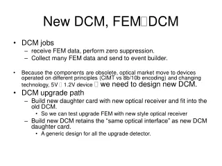
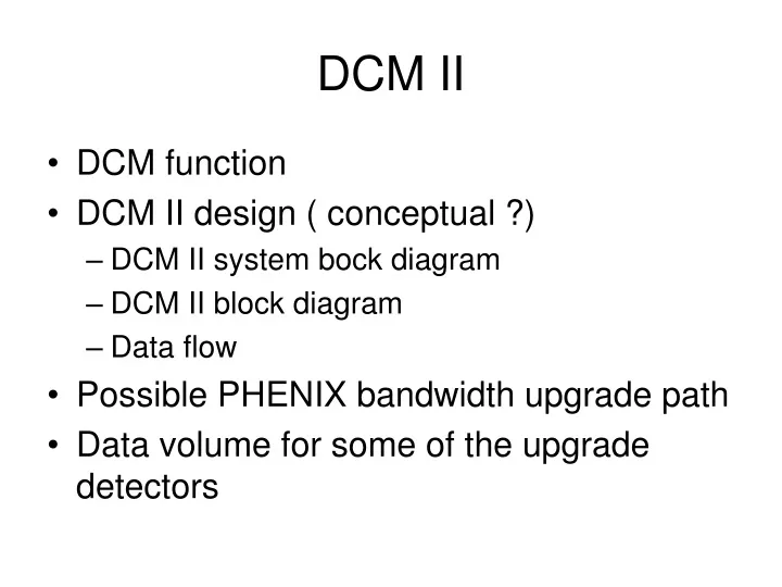
DCM II • DCM function • DCM II design ( conceptual ?) • DCM II system bock diagram • DCM II block diagram • Data flow • Possible PHENIX bandwidth upgrade path • Data volume for some of the upgrade detectors
DCM II Function • Collect FEM data • Zero suppressed data • Data Error/ Event Alignment checking • Alignment checking via L1 data or/and adjacent data link • Pocketsized data • Possibility for data processing • First stage of event building • we need to handle possible link errors associate with increasing radiation. It may not be practical any more to stop run when one link drop out during the run.
DCM II system diagram Custom Backplane BUSY DOWNLOAD READBACK DATA L1 INTERFACE Partitioner II DCM II DCM II DCM II GTM L1 Download/reback 40Mbytes/sec DCM data link 640 Mbytes/sec DCM II/ JSEB II link 6.4 Gbits/sec. FEM/DCM 16bits/80MHz clock FEM JSEB II JSEB II PC SEB PC The DCM II system is similar to the DCM – the JSEB II will use PCI express bus (2.5 Gbits/sec/per lane) in PC. The new JSEB will have by-directional optical links.
Conditions for building DCM II • We will use new optical serializer/de-serializer for the FEM to DCM II link. • a) faster speed, b) more reliable protocol and c) GLINK is probably will be phase out some point in the future • Penalty is the data word is only 16 bits wide. • We will use FPGA to replace DSP function. • The old zero suppression code is running at speed while DSP program still being improving • FPGA can process data in parallel with pipeline operation. • It is easier to build speed into the system than the increasing buffer memory size • New chip set just run faster… • Running faster require less memory to buffer the data • DCM I is using VME crate with semi-custom dataway. • The VME market is getting smaller, crate controller run slower than PC and cost more (5K vs 1K ?) and require special operating system (for example VxWork) • Except for busy fanout, nobody else use the DCM crate. • VME64X backplane mechanical structure has problem bend pins • The DCM II will use complete custom dataway with proper 2mm HM and 2mm HM ZD connectors for keying. • We will use PC + DCM interface board to replace VME crate controller
DCM II Block Diagram ALTERA STRATIX I EP1S30 8 optical links per DCM 5 event buffer Event buffer 320 Mbytes/sec Optics+ De-serializer Zero sup- pression ALTERA STRATIX II EP2S60 L1 data MUX 5 event buffer Event buffer Optics+ De-serializer Zero sup- pression receiver buffer Data link in Alignment FEM DCM link 80 MHz 16 bits/word 1.6Gbits/sec 8b/10b encoding method choose Ti’s TLK2501 as de-serializer STRATIX has 2 Mbits for event data buffer 1 Mbits for processing buffer 30K logical element old DCM has 1K Logical element per optical link Data processing Event Buffer 640 Mbytes/sec MUX Data link out receiver buffer 5 event buffer Event buffer Optics+ De-serializer Zero sup- pression MUX STRATIX II has 1 Mbits for event data buffer 1.5 Mbits for processing buffer 20K - 60 K logical element faster than STRATIX I 5 event buffer Event buffer Optics+ De-serializer Zero sup- pression Alignment ALTERA STRATIX I EP1S30
Power Possible floor plan for the DCM II De-serializer High speed ZD connector FPGA To merge data Control/ download Optical transceiver Zero Suppression FPGA
DCM II parameters • FEM link run 80MHz 16 bits mode • 50 microsec/12.5ns = max 4K words per events • Assume at least factor 10 zero suppression factors. • 8 optical ports per DCM. • We could use half the optical port if detector has less than factor 10 zero suppression rate. • The available buffer size will increase by factor 2 • Input 8*80 Mwords (16 bits per word)/sec, max output rate is 160 Mwords (32 bits/per word) /sec. • Large data buffer at Partition III, ½ MWords. • Paritioner III to JSEB II link will be running at around 4-6 Gbits/sec. • DCM II board size currently is 6Ux160mm, slightly smaller than size of A4 paper.
JSEB II JSEB II interface to PC through PCI express bus. The PCI express has 2.5 Gbits/sec per lane. Max. 12 lanes per interface. The current local bus to PCI express bus only support one lane. Serve both slow control path and DCM II path. Use optical cable to both paths. Smaller size and less distance constrain. DCM data optical Serializer De-serilaizer FPGA Altera Arria Download Control/ Slow readback 4 lanes 10 Gbits/sec
Future DAQ upgrade choices • WE have the following choices • A) Restore the bandwidth by factor of 2 • Max 10KHz Max 20KHz. • B) Make sure everything could run up to 10KHz trigger rate. • C) Make everything run as fast as it can without big investment.
Current DCM count • 74 DCM with FE1 ( 20bits wide data word). • TEC 42. • PC 10. • DC 20. • MuID 2, • 93 DCM with FE2(16 bits wide data word). • Muon Tracking 56. • EMCAL 24. • RICH 4. • other detectors 9. • Exclude RXN, HBD and test stands. • Excluding spares.
Cheapest (minimum change) solution to improve bandwidth Matt’s 6/23/07 mail • Packet Mean Sigma Detector • 22006 318.2 230.9 HBD • 3145 294.4 49.1 DC • 3011 288.6 41.8 DC • 3125 288.3 42.3 DC • 22011 273.4 198.9 HBD • 23001 258.0 0.0 RXNP • 22010 238.9 209.8 HBD • 21031 233.0 86.3 MPC • 21032 226.8 74.8 MPC • 21022 219.2 85.0 MPC • 1003 215.0 0.0 BBC • 1002 215.0 0.0 BBC Comments: Next year we will have rebuilt HBD, data size could be different. We could also double no. of HBD fibers or reduce number of samples. Can we cover the GLINK optical system to 8b/10b system? readout through DCM II If we solve the problem with DC, MPC, RXNP and BBC, will DAQ run fast enough? Bank swapping run at 6.4KHz Without HBD and DC
Solution to achieve 10KHz rate in DCM (even with non-zero suppressible data) • Reuse the DCM daughter cards • Build a new card with DCM II backend architectures. • use FPGA to merge 4 inputs to one 320 Mbytes/sec link. • Need to build 180+ new cards or 720+ links • Assume $200-$300 per links + EDIA etc.
Possible upgrade path to restore the full trigger rate • What we know • DCM run $1K per link. • 16 bits word size for FE2, 20 MHz data rate. • 20 bits word size for FE1, 40 MHz date rate. • DCM II is about .5K - .7K • 16 bits word size, 80 MHz data rate. • The DCM II is about factor 4 faster and about factor 2 cheaper in price compare to DCM equib with FE2. • As time goes by, it will harder and harder to rebuild DCM. • Possible methods to restore the bandwidth • Rebuild some detector with 16 bits readout mode to DCM II to free up old DCM boards for other detectors. • Use those free up DCM boards to readout other old detectors.
Possible upgrade path to restore the full trigger rate (II) • Muon Tracking use 56 DCM with FE2. • The cost double DCM for MuTr will be 224K + cost on MuTr FEE copper to fiber crate. • The cost to readout MuTr completely through DCM II will be readout through 56 *4 ports per DCM * factor 2 / 4 (number data packet could stuff through DCM II) = 112 optical ports • Cost will be .6k*112= 67.2K + cost plus the cost of rebuild MuTr copper to fiber crates. • This would free up 56 FE2 DCM boards. • To free up FE1 DCM is more complicated. Possible solutions could include • Rebuild DC FEM optical output interface. • Build optical data format exchange board. • GLINK in and 8/10b optical out.
VTX barrel pixel • Pixel data • 5 header words +4 SPIRO words +5 trailer word • 2 groups 2048 16 bits data word (y/n, 1bits per pixel) • Pixel calculated occupancy for Au-Au central is 0.53% and .16%. • assume 1% noise rate --- estimate zero suppress data volume • Split data into 8 bits group, for un-zero byte, attached with 6 bits label to form 16 bits data word, add additional word every 64 bytes. • 1 % occupancy mean => every 64 bytes will have 7 16 bits word • So average data volume for pixel data is = (7+1)*64 groups * 2 sets / (32/16 packing) = 512 words +7 = 519 words compare to 4.1K words un-zeo suppressed data volume • 8 optical fiber per DCM => 4136 words 32 bits word per events => 41Mwords per sec for 10 KHz trigger rate. • Pixel has 60 fibers.
VTX barrel strips • Silicon strips is through SVX chip. 128 channel per SVX 4. 12 SVX per RCC. 5/6 RCC per ladder. 18 ladder for R3 and 26 ladder per R4. SVX has one board zero suppression (one threshold level). • ~4.5% occupancy in R3 and ~2.5% occupancy in R4. Assume 1% noise. • For every RCC, there are 2 “identify” words. For every SVX 4 words there is 1 address word. 10 header+trailer word per packet. • Data size for Au-Au central • = 10+{5 (RCC) *2 + 60(SVX)* (1 header + 7 data words) (~128*.0.055)}/2 = 255 32 bits words per ladder R3 • = 10+{6 (RCC) *2 + 72(SVX)* (1 header + 5 data words) (~128*.0.035)}/2 = 232 32 bits words per ladder R4 • Total data volume is • (255*18+232*26) =10.6K words per Au-Au events.
FVTX • Channel counts = (73.7+160+160+160)K =553.7K, 48 wedges per disk. • Assume one fiber per wedge. • 3 (5) bits FADC per channel = only readout hit channel = 1 16 bits word per channel • 2.8 % occupancy in au-au central plus 1 % noise. • Data volume = 3.8% * 553.7K channel = 21K 16 bits words + all header + address words…
RPC, NCC and HBD • RPC measures time. The RPC2 and RPC3 should have similar hit rates as Muon ID, 20 hits for Au-Au mini bias. We need to look at RPC1 occupancy for Au-Au events • NCC has 2 EM, 1 HAD sections plus 2 strips plans readout by SVX4. • EM and HAD readout through multi-samples ADC. • I would expect data volume at factor 2 above the FVTX > 21K words • HBD has 2.3K channel. • The data word per channel is 7. Without zero suppression, the data volume is 16K. The problem is not size of total events but data word per fiber. One could double number fibers or only output summary information.