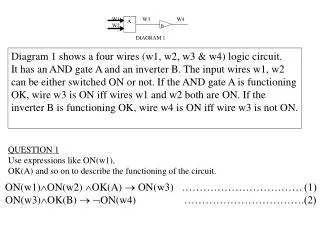
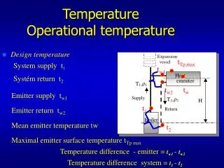
Download
1 / 15
150 likes | 281 Views
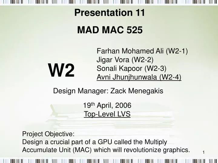
Presentation 11 MAD MAC 525. Farhan Mohamed Ali (W2-1) Jigar Vora (W2-2) Sonali Kapoor (W2-3) Avni Jhunjhunwala (W2-4). W2. Design Manager: Zack Menegakis. 19 th April, 2006 Top-Level LVS. Project Objective:

E N D
Presentation 11 MAD MAC 525 Farhan Mohamed Ali (W2-1)Jigar Vora (W2-2)Sonali Kapoor (W2-3) Avni Jhunjhunwala (W2-4) W2 Design Manager: Zack Menegakis 19th April, 2006 Top-Level LVS Project Objective: Design a crucial part of a GPU called the Multiply Accumulate Unit (MAC) which will revolutionize graphics.
MAD MAC 525 Status: • Project chosen • Specifications defined • Architecture • Design • Behavioral Verilog • Testbenches • Verilog : Gate Level Design • Floor plan • Schematics and Analog Verifications • Layout of basic gates and small modules • Top level layouts, Extractions, LVS, Simulations • Full Chip Layout completed and LVSed To be done • Simulations and full chip verification
Block Diagram Input Input 16 Input 16 16 5 RegArray A RegArray B RegArray C 10 10 5 10 5 Multiplier Exp Calc Align 1 5 22 14 35 Control Logic & Sign Dtrmin Leading 0 Anticipator Adder/Subtractor 36 4 Normalize 14 1 5 Round Reg Y 1 10 5 15 16 Output 1 Ovf Checker
Full Chip Layout Exponent Multiplier Zero Align Adder O v f N o r m a l i z e R o u n d
Design Specifications • Register-to-register delay (worst case)= 2.25ns • Long buses are all buffered (not tested yet) • Estimated clocking speed = 400MHz • Height by width = 193.86 um * 301.545 um • Area = 58,458 um^2 • Aspect ratio = 1:1.55 • Total Transistor density = 0.22