Download
1 / 2
20 likes | 225 Views
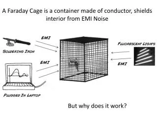
A/D. Digital Logic. A/D. Analog/RF. A/D. Noisy Substrate. Si. Cu. 12 µ m. Reference. Faraday Cage. Substrate thickness=77 µm Separation dist.=100 µm Via separation=10 µm Via diameter=10 µm. Air. At 100 µ m distance, on average:. 1 GHz: 41 dB improvement

E N D
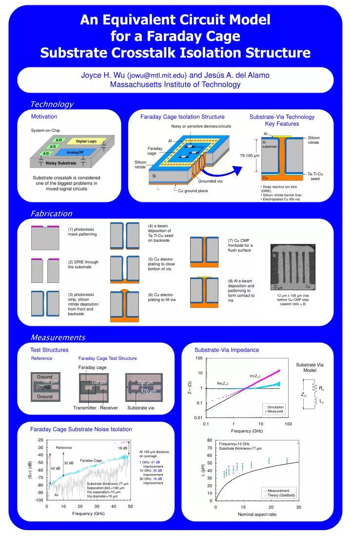
A/D Digital Logic A/D Analog/RF A/D Noisy Substrate Si Cu 12 µm Reference Faraday Cage Substrate thickness=77 µm Separation dist.=100 µm Via separation=10 µm Via diameter=10 µm Air At 100 µm distance, on average: 1 GHz: 41 dB improvement 10 GHz: 30 dB improvement 50 GHz: 16 dB improvement Simulation Measured An Equivalent Circuit Model for a Faraday Cage Substrate Crosstalk Isolation Structure Joyce H. Wu (jowu@mtl.mit.edu) and Jesús A. del Alamo Massachusetts Institute of Technology Technology Motivation Faraday Cage Isolation Structure Substrate-Via Technology Key Features Noisy or sensitive devices/circuits System-on-Chip Al Silicon nitride Al Si substrate Faraday cage 75-100 µm Silicon nitride Ta-Ti-Cu seed Si Substrate crosstalk is considered one of the biggest problems in mixed-signal circuits Cu Grounded via • Deep reactive ion etch (DRIE) • Silicon nitride barrier liner • Electroplated Cu fills via Cu ground plane Fabrication (4) e-beam deposition of Ta-Ti-Cu seed on backside (1) photoresist mask patterning (7) Cu CMP frontside for a flush surface (5) Cu electro-plating to close bottom of via (2) DRIE through the substrate (8) Al e-beam deposition and patterning to form contact to via (3) photoresist strip, silicon nitride deposition from front and backside (6) Cu electro-plating to fill via 12 µm x 100 µm vias before Cu CMP step (aspect ratio= 8) Measurements Test Structures Substrate-Via Impedance Reference Faraday Cage Test Structure Substrate Via Model: Faraday cage Im(Z11) Ground 100 µm 100 µm 200 µm Re(Z11) Signal Rv 70 µm Z11 Ground Lv Transmitter Receiver Substrate via Faraday Cage Substrate Noise Isolation
Rr R1 = 2 Reference Faraday Cage 100-µm pad separation Simulation Measured Simulation Measured Simulation Measured Simulation Measured 100-µm Reference 200-µm 100-µm Faraday Cage 200-µm Equivalent Circuit Model Reference Structure Reference Structure with center split Rr R1 R1 Cpad Cpad Cpad Cpad R2 R2 R2 R2 C1 = 2Cr Cr C1 C1 R3 C3 R3 C3 R3 C3 R3 C3 Rr = 5 k Cr = 3 fF R1 = 2.5 k C1 = 6 fF 100-µm transmitter-receiver separation 100-µm transmitter-receiver separation Model unchanged by split Add series Rv and Lv of via 100-µm transmitter-receiver separation Faraday Cage Structure Reference R1 R1 Rv=1 kΩ Lv=500 pH Cpad Cpad R2 R2 Change only Rv and Lv to evolve from reference to Faraday cage structure Rv=250 Ω Lv=200 pH Rv=70 Ω Lv=70 pH C1 C1 Faraday Cage Rv R3 C3 R3 C3 Rv=25 Ω Lv=50 pH Lv R1 = 2.5 k C1 = 6 fF Simulations Comparison of Measurement and Simulation Equivalent circuit lumped-element values Imag Measured Simulation Real S21 • Simple model matches data well (including real and imaginary S21) • Range of Rv and Lv consistent with measured values • Spread of Rv and Lv of substrate via accounts for spread in S21 of Faraday cage Conclusions Increase Tx-Rx separation distance Increase via spacing • Developed a simple, lumped-element equivalent circuit model • Model matches experimental data into mm-wave regime • Model will be useful to evaluate substrate noise isolation schemes in actual circuits Rv=45 Ω Lv=30 pH Rv=20 Ω Lv=30 pH 70-µm via spacing 10-µm via spacing • Increasing via spacing reduces substrate noise isolation • Effectiveness of Rv-Lv shunt is reduced due to fewer vias • Only need to increase Rv-Lv values for larger via spacing • Increasing pad separation reduces substrate noise • R1 and C1 to account for greater pad separation