Download
1 / 15
150 likes | 264 Views
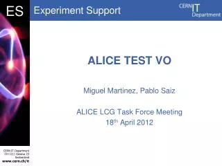
Test of One ALICE Pixel Assembly in the NA48 Beamline. Wednesday, June 16 - Thursday, June 17, 2004. Chip and Sensor Characteristics. P. Riedler/CERN ALICE. ALICE Pixel - Test Beam Setup.

E N D
Test of One ALICE Pixel Assembly in the NA48 Beamline Wednesday, June 16 - Thursday, June 17, 2004 Chip and Sensor Characteristics P. Riedler/CERN ALICE
ALICE Pixel - Test Beam Setup ALICE SPD carried out test beams in 2001, 2002, 2003 in proton and heavy ion beams at the SPS using a specially developed DAQ system: • One plane installed for NA48: • 1 ALICE assembly • 1 DAQ adapter card • 30 m DAQ cables • 30 m JTAG control cables • LV and HV power supplies • VME crate with r.o. module (Pilot) and JTAG controller • JTAG multiplexer • MXI interface to PC • ALICE PTS software (LabView) • PC remotely controlled from NA48 control room ALICE TB 2002 setup with 3 DAQ planes and 5 assemblies P.Riedler/CERN
Giorgio Stefanini Petra Riedler PJAS Peter Chochula Mike Burns Alex Kluge Michel Morel Fadmar Osmic DOCT ALICE pixel team members helping with the preparations and the test: P.Riedler/CERN
Schematic of a Hybrid Silicon Pixel Detector Readout Chip Bump Bonds Sensor P.Riedler/CERN
13.5 mm 15.8 mm ALICE Pixel Chip • 0.25µm CMOS process • radiation tolerant design • clocked at 10MHz • 8192 pixel cells with digital • output • ~100 µW/channel • ~1000 e- mean threshold • (~200 e- RMS • ~13 mio. transistors • 1200 ALICE Pixel Chips will be used in the SPD (Silicon Pixel Detector) 50 µm x 425 µm pixel cell P.Riedler/CERN
ALICE chip wafer Native thickness 725 µm Produced by IBM Wafer material: “electronics grade” 8 in. silicon wafers Each chip needs to be tested before the wafer is sent for bump bonding. According to a KGD (Known Good Die) map only those chips that fulfill all test criteria are used for bump bonding. KGD yield on ALICE chip wafer: ~55% (86 chips per wafer in total) P.Riedler/CERN
ALICE Sensor 1 ALICE silicon sensor is connected to 5 ALICE readout chips via 40960 bump bonds Sensor thickness: 200 µm Wafer material: High resistivity FZ 5 in. wafer Pixel size: 50µm x 425µm P.Riedler/CERN
Pb-Sn Bump Bond Bump Bonds 25µm P.Riedler/CERN
J. Salmi/VTT Presentation at BOND’03 workshop, CERN, June 2003 Material Budget • Requirements for ALICE: • <1 % X0 total per pixel layer • e.g. • 200 µm thick sensors • Chip wafers thinned to 150µm after bumping • Multilayer kapton bus with Al P.Riedler/CERN
Thinned Chip Wafers (10-30 µm) P. Mikulik et al, http://www.xray.cz/xray/csca/kol2002/doc/petr_mikulik.htm P.Riedler/CERN
Radiation Effects in Silicon Surface Damage Bulk Damage Electronics Detectors Full bulk is sensitive to passing charged particles Sensitive components are located close to the surface P.Riedler/CERN
Estimation of the Radiation Effects for Future NA48 • VERY PRELIMINARY! Fluence: Assuming 5000 spills/day, 50MHz particles/cm2/spill and a spill length of 4.8s: 1.2E12 particles/cm2 per day Assuming pion beam: feq= kf k…hardness factor (9GeV pions:3.6, flat dist.) feq=4.32E12 (1 MeV neutrons)/cm2 per day Assuming 100 days of running: feq= 4.32E14 (1 MeV neutrons)/cm2 per run • >> Leakage current, depletion voltage, signal, operating conditions,…. • Dose: 4.32E14/(6.24E9/(1.66 MeV g-1 cm2))=114kGy=11.4Mrad P.Riedler/CERN
Single Chip ALICE Assembly tested in NA48 • 150µm thick ALICE chip • 200µm thick sensor • Mounted on a thin test-PCB • Vfd=15V • Vop=30V, 50V • 8192 pixels • Produced 2003, tested in • ALICE p-TB 2003 Sensor Chip P.Riedler/CERN
Timeline of the Test in NA48 • Preparations: • May/June 2004: • Installation of one ALICE SPD testbeam plane in the NA48 lab • Beam: • Wednesday, June 16: • Installation in the beamline at the position of KABES2 • Begin of data taking • Thursday, June 17: • End of beam at about 14.00, reinstallation of KABES2 • ~140 MB data taken (SPD TB 2003, HI run, 3 weeks: 3GB) P.Riedler/CERN
More on the tests: see talk by M. Martini P.Riedler/CERN