Download
1 / 48
480 likes | 556 Views
LZRW3 Data Compression Core. mid presentation Part A Project Netanel Yamin & by: Shahar Zuta Moshe porian Advisor: Dual semester project November 2012. Contents. Project Overview Project goals Requirements Architecture Micro architecture Problems & solutions Conclusions

E N D
LZRW3 Data Compression Core mid presentationPart AProject Netanel Yamin & by: Shahar Zuta Moshe porianAdvisor: Dual semester project November 2012
Contents • Project Overview • Project goals • Requirements • Architecture • Micro architecture • Problems & solutions • Conclusions • Testability • Methodology • Schedule
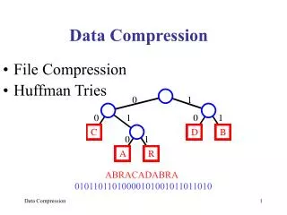
algorithm overview LZRW3 OUTPUT FILE [----][-----]-[-------][-----------][----] INPUT FILE ------------------------------------------------------- LZRW3 COMPRESSOR Literal items ONLY GROUPS OF ITEMS (literal/Copy) A copy item consists of two bytes that represent from 3 to 18 bytes. literal item consist of one byte which represents himself
mechanism LZRW3 “L.I“ stands for “ Literal Item “ Offset Output 4095 Exp L.I XXX UUU INDEX res L.I UUU NOTE: The next 3 byte should be “x p r” , then “ p r e “ and only then “r e s”, we did’nt demonstrate all the actions for simplicity. XXX HASH FUNCTION YYY ZZZ 0 r e s E x p INPUT FILE: Exp res sio n_c omp res s i o n demonstration _ 3 0 Offset value=
mechanism LZRW3 Output Offset 4095 Exp L.I YYY ZZZ INDEX res L.I 0 UUU sio L.I 3 XXX HASH FUNCTION n_c L.I YYY ZZZ 0 n c i _ s o INPUT FILE: Exp res sio n_c omp res s i o n demonstration _ 6 Offset value= 9
mechanism LZRW3 Output Offset 4095 Exp L.I INDEX res L.I 0 UUU sio L.I 3 XXX HASH FUNCTION n_c L.I 9 YYY omp L.I ZZZ 6 0 o m p INPUT FILE: Exp res sio n_c omp res s i o n demonstration _ 12 Offset value=
mechanism LZRW3 Output Offset 4095 Exp L.I XXX INDEX 12 res L.I 0 UUU sio L.I 3 “C.I“ stands for “ Copy Item “ XXX HASH FUNCTION n_c L.I 9 YYY omp L.I 6 ZZZ 3 4 5 1 2 XXX C.I 3+ 0 0 r e s INPUT FILE: Exp res s i _ o n comp res s _ i o n demonstration 1 2 3 15 Offset value=
START FWD 1 byte Hash 3 bytes FWD 3+ Length bytes index Hash table [index] Enter offset O.F.- Literal item empty filed Get offset yes Same 3 bytes more same bytes no yes Length++ O.F.- Copy item
Project Goals • Implementation of LZRW3 data compression algorithm • Implementing strong debugging capabilities via GUI
Requirements • VHDL implementation • DE2 development board that features an Altera Cyclone II FPGA • FPGA – Host communication via UART protocol • Use internal memory on FPGA, no interface to external memory • Adapted to data templates of 2Kbyte to 32Kbyte • High performance- data transfer of 1Gbps
Requirements • VHDL implementation • XUPV5development board that features an Xilinx Virtex-5FPGA • FPGA – Host communication via UART protocol • Use internal memory on FPGA, no interface to external memory • Adapted to data templates of 2Kbyte to 32Kbyte • High performance- data transfer of 1Gbps
Architecture XILINX VIRTEX 5 ON XUVP505 BOARD Rx PATH UART GUI LZRW3 COMPRESSOR CORE INPUT BLOCK memory Tx PATH COMPRESSED FILE memory UART
Architecture XILINX VIRTEX 5 ON XUVP505 BOARD Rx PATH UART GUI LZRW3 COMPRESSOR CORE INPUT BLOCK memory Tx PATH COMPRESSED FILE memory UART
LZRW3 COMPRESSOR CORE Lzrw3_go LZRW3 COMPRESSOR CORE Lzrw3_busy Lzrw3_mode Lzrw3_done Lzrw3_output_group_size (4..0) data_input_byte (7..0) data_input_valid data_output_bytes(13..0) End_of_file data_input_taken data_output_valid data_output_taken clk data_output_last reset
STAGE 1 – three bytes buffer 3BYTES BUFFER enable New_byte(7..0) Newer_byte(7..0) Mid_byte(7..0) Older_byte(7..0) reset clk
STAGE 2- hash function enable HASH FUNCTION Newer_byte(7..0) middle_byte(7..0) Table_index(11..0) older_byte(7..0) reset clk
TABLE INDEX = (((40543*(((*(PTR))<<8)^((*((PTR)+1))<<4)^(*((PTR)+2))))>>4) & 0xFFF)PTR pointes to the first byte . TABLE INDEX range: 0 to 4095. HASH FUNCTION
STAGE 3 – hash table HASH TABLE enable Offset(19..0) Data_out_valid Table_index(0..11) Offset counter Current_offset(19..0) clear reset clk
Stage 3- illustration Valid bits 21 bits Offset counter Offset counter 0 0 Current_offset 0 DATA_ IN 0 Offset OFFSET OFFSET 1 1 4096 rows 1 Data_out_valid INDEX 0 1 0 ADDRESS 1 1 0
Stage 4 implementation • Input file memory should supply three byte at the same time.
How to choose bank when byte arrives ? MODULE and DIVIDE are NOTsyntesisable
SOLUTION • Instead of counting in stage 3 and divide in stage 4, we incerment by one only after three clock cycles. • In this configuration we expand the offset by 2 bits (tagging) to select the the data need to write into. • Hash table size now is 4096 x (19+2) . OFFSET TAG 1001010101001110011 10 19 bits 2 bits
Solution costs (mem units) • Memory usage At stage 3 from synplify_pro: same as before. • LUT usage: 36Kbit
clk Tentative Next address Input file memory banks clk STAGE 4 Illustration TENT D B clk C Addresses alignment X Y Z 1 offset Bank 0,1,2 addresses 0 0 clk TAG indicate the banks bytes order counter 3401 Item_length_p 0 Tentative_taken Offset_valid Comprison_valid comparator Continue 1 0 0 1 1 0 Compare_success Tentative_tag 1 TAG Compare_success_P Offset_tag 0 clk B A Older_byte_P clk Offset_valid D C Newer B Mid C A Older B Index INDEX
clk Tentative Next address Input file memory banks clk STAGE 4 Illustration clk Addresses alignment T D C 1 offset Bank 0,1,2 addresses 1 clk counter Item_length_p 0 Tentative_taken Offset_valid Comprison_valid comparator Continue 0 0 Compare_success Tentative_tag 1 TAG Compare_success_P Offset_tag 0 clk C Older_byte_P clk Offset_valid E Newer Mid D Older C Index INDEX
Problem(1) in stage 4, at first we implemented the counter that counts the number of successful comparisons in the comparator which is made of an asynchronous process. It passed simulations but was not synthesizable.
Solution(1) we’ve changed the architecture of the units so the counter is implemented in a synchronous unit, it receives a signal from the asynchronous comparator if the comparison was successful and responds accordingly.
Problem(2) in stage 4, in order to perform the comparison of the current 3 bytes in the pipe and three bytes from the RAM memory we need to extract three following bytes from different addresses at one clock period.
Solution(2) we distributed the one memory we had into 3 RAM memory banks which contains following addresses so in case we want to extract 3 following bytes from the memory we’ll extract one byte from each bank.
Problem(3) in stage 4, the current pipe bytes that arrive the comparator are arranged in their arrival order but the three bytes withdrawn from the banks aren’t necessarily arranged in the right order.
Reading configurations 1. SAME ADDRESES
Reading configurations 2. DIFFERENT ADDRESS
Reading configurations 3. DIFFERENT ADDRESS # 2
ׂ(3)Solution We used the TAG that represented the extracted bytes addresses to determine which extracted byte will be compared with which current piped byte.
Problem(4) In stage 4, the RAM memory banks need to have the next address to extract on the next clock before the end of the current clock.
(4)Solution We created two units that will contain the next two possible addresses (tentative address unit or address align unit).
Conclusions • Writing code for synthesis is different from writing code for simulation. • In asynchronousimplementation all the signals need to be in the sensitivity list. • Reset should not pass through any logic. • Think hardware when writing VHDL code for synthesis. • Keep on simplicity to achieve more flexibility.
Assert the comparison and report to console Testability Synthesisable Hash Function Block 2048 Random input generator A B C A B C Unsynthesisable Simulation Function 2048 Input file
Methodology • Stage data flow review. • Writing VHDL code. • Writing VHDL testbench. • Code review and debugging. • Synthesis check- synplify. • Check RTL view. • Check CLK constraints. • Commit SVN folders and update data flow if needed. • Next stage data flow review. Simulation & debugging