1 / 39

Chapter 4 Bipolar Junction Transistors

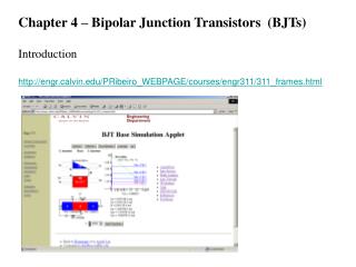
Chapter 4 Bipolar Junction Transistors Ebers-Moll Model -Table 4.2 Input and Output Characteristics SPICE parameters ----to I-V curvers Regions of Opertion Biasing the BJT Bias Stability Small Signal Models Single Transistor Amplifiers BJT I-V Relationships Output characteristics

paul
Download Presentation

Chapter 4 Bipolar Junction Transistors

An Image/Link below is provided (as is) to download presentation Download Policy: Content on the Website is provided to you AS IS for your information and personal use and may not be sold / licensed / shared on other websites without getting consent from its author. Content is provided to you AS IS for your information and personal use only. Download presentation by click this link. While downloading, if for some reason you are not able to download a presentation, the publisher may have deleted the file from their server. During download, if you can't get a presentation, the file might be deleted by the publisher.

E N D

Presentation Transcript


  1. Chapter 4Bipolar Junction Transistors

  2. Ebers-Moll Model -Table 4.2 Input and Output Characteristics SPICE parameters ----to I-V curvers Regions of Opertion Biasing the BJT Bias Stability Small Signal Models Single Transistor Amplifiers BJT I-V Relationships

  3. Output characteristics B-E and C-B Junctions

  4. Forward Bias

  5. Ebers-Moll for computer/hand use 4.13

  6. Ebers-Moll for computer/hand use

  7. Example Using Table 4.2 Eqs

  8. SPICE Example to VERIFY Table 4.2

  9. Generating OTC Curves Ex 4.14 pp239

  10. Circuit Modeling of Regions

  11. Physical Base Currents

  12. Example Region chk 4.12

  13. Simple BJT Switch 4.12

  14. Operating and Biasing Constraints

  15. Fixed Biased Circuit pp236-54

  16. Temperature Effects and RE pp239

  17. Analysis of Transistor DC Bias

  18. Self Biased with RE

  19. Self Biased with RE

  20. Self Biased Example

  21. Example Con’t

  22. Bias Stability

  23. Collector Current Variation

  24. Collector Current Variation

  25. Collector Current Variation

  26. Example

  27. PSPICE

  28. Small Signal Model pp 256

  29. Small Signal Model pp257

  30. Small Signal Model Gain pp259-60 See Ex 4.9 Application of ss models 

  31. Application of Small Signal Model pp262

  32. Small Signal Model with Re pp285

  33. Small Signal Model with Re pp285

  34. Common Collector pp290

  35. Common Collector Con’t

  36. Small Signal Model Con’t Add Cs

  37. Small Signal Model Cuttoff f

  38. Small Signal Model Cuttoff f See Fig 4.73 pp 325 also. This slide presents a very key concept. In practice in broad band amplifier design one CANNOT expect to apply a transistor beyond T…. 0 dB

  39. Small Signal Model EX 4.76This is what its is about Understand and know for exam!!!

More Related