Download
1 / 136
1.38k likes | 1.72k Views
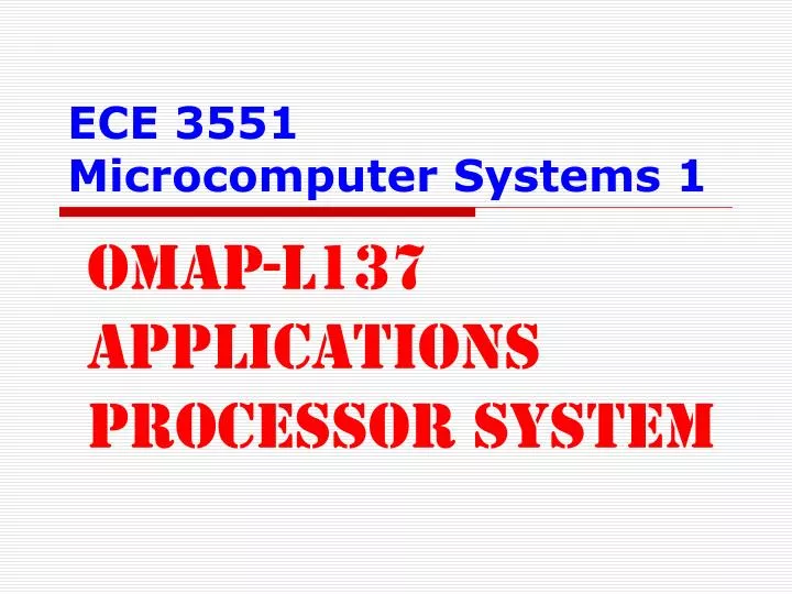
ECE 3551 Microcomputer Systems 1. OMAP-L137 Applications Processor System. Highlights. Dual Core SoC 375/456-MHz ARM926EJ-S™ RISC MPU 375/456-MHz C674x VLIW DSP TMS320C674x Fixed/Floating-Point VLIW DSP Core Enhanced Direct-Memory-Access Controller 3 (EDMA3) 128K-Byte RAM Shared Memory

E N D
ECE 3551 Microcomputer Systems 1 OMAP-L137 Applications Processor System
Highlights • Dual Core SoC • 375/456-MHz ARM926EJ-S™ RISC MPU • 375/456-MHz C674x VLIW DSP • TMS320C674x Fixed/Floating-Point VLIW DSP Core • Enhanced Direct-Memory-Access Controller 3 (EDMA3) • 128K-Byte RAM Shared Memory • Two External Memory Interfaces • Three Configurable 16550 type UART Modules • LCD Controller Veton Këpuska
Highlights • Two Serial Peripheral Interfaces (SPI) • Multimedia Card (MMC)/Secure Digital (SD) • Two Master/Slave Inter-Integrated Circuit • One Host-Port Interface (HPI) • USB 1.1 OHCI (Host) With Integrated PHY (USB1) Veton Këpuska
OMAP-L137 Applications Processor System Describes the System-on-Chip (SoC) system. The SoC system includes TI’s standard TMS320C674x and several blocks of internal memory (L1P, L1D, and L2): Power and sleep controller (PSC) Power management System configuration (SYSCFG) module ARM interrupt controller (AINTC) Boot considerations • ARM subsystem • DSP subsystem • System interconnect • System memory • Memory protection unit (MPU) • Device clocking • Phase-locked loop controller (PLLC) Veton Këpuska
Outline Veton Këpuska
Outline Veton Këpuska
Introduction • The OMAP-L137 Applications Processor contains two primary CPU cores: • an ARM RISC CPU for general-purpose processing and systems control; and • a powerful DSP to efficiently handle communication and audio processing tasks. • The OMAP-L137 Applications Processor consists of the following primary components: • ARM926 RISC CPU core and associated memories • DSP and associated memories • A set of I/O peripherals • A powerful DMA subsystem and SDRAM EMIF interface Veton Këpuska
Outline Veton Këpuska
Block Diagram Veton Këpuska
Outline Veton Këpuska
DPS Subsystem • The DSP subsystem (DSPSS) includes TI’s standard TMS320C674x module and several blocks of internal memory: L1P, L1D, and L2. Veton Këpuska
Outline Veton Këpuska
ARM Subsystem • The ARM926EJ 32-bit RISC CPU in the ARM subsystem (ARMSS) acts as the overall system controller. • The ARM CPU performs general system control tasks, such as system initialization, configuration, power management, user interface, and user command implementation. Veton Këpuska
Arm Subsystem Veton Këpuska
Arm Subsystem Veton Këpuska
Introduction • The ARM subsystem consists of the following components: • ARM926EJ-S - 32-bit RISC processor • 16-kB Instruction cache • 16-kB Data cache • Memory management unit (MMU) • CP15 to control MMU, cache, etc. • Java accelerator • ARM Internal Memory • 8 kB RAM • 64 kB built-in ROM Veton Këpuska
Introduction • Embedded Trace Module and Embedded Trace Buffer (ETM/ETB) • Features: • The main write buffer has a 16-word data buffer and a 4-address buffer • Support for 32/16-bit instruction sets • Fixed little-endian memory format • Enhanced DSP instructions Veton Këpuska
Introduction • The ARM926EJ-S processor is a member of the ARM9 family of general-purpose microprocessors. • The ARM926EJ-S processor targets multi-tasking applications where full memory management, high performance, low die size, and low power are all important. • The ARM926EJ-S processor supports the 32-bit ARM and the 16-bit THUMB instruction sets, enabling trade off between high performance and high code density. Veton Këpuska
Introduction • This includes features for efficient execution of Java byte codes and providing Java performance similar to Just in Time (JIT) Java interpreter without associated code overhead. • The ARM926EJ-S processor supports the ARM debug architecture and includes logic to assist in both hardware and software debugging. Veton Këpuska
Introduction • The ARM926EJ-S processor has a Harvard architecture and provides a complete high performance subsystem, including the following: • An ARM926EJ-S integer core • A memory management unit (MMU) • Separate instruction and data AMBA AHB bus interfaces Veton Këpuska
Introduction • The ARM926EJ-S core includes new signal processing extensions to enhance 16-bit fixed-point performance using a single-cycle 32 × 16 multiply-accumulate (MAC) unit. • The ARM core also has 8 kB RAM (typically used for vector table) and 64 kB ROM (for boot images) associated with it. • The RAM/ROM locations are not accessible by the DSP or any other master peripherals. Furthermore, the ARM has DMA and CFG bus master ports via the AHB interface. Veton Këpuska
Arm Subsystem Veton Këpuska
Operating States/Modes • The ARM can operate in two states: ARM (32-bit) mode and Thumb (16-bit) mode. • The ARM926EJ-S processor is switched between ARM mode and Thumb mode using the BX instruction. • The ARM can operate in the following modes: • User mode (USR): Non-privileged mode, usually for the execution of most application programs. • Fast interrupt mode (FIQ): Fast interrupt processing Veton Këpuska
Operating States/Modes • Interrupt mode (IRQ): Normal interrupt processing • Supervisor mode (SVC): Protected mode of execution for operating systems • Abort mode (ABT): Mode of execution after a data abort or a pre-fetch abort • System mode (SYS): Privileged mode of execution for operating systems • Undefined mode (UND): Executing an undefined instruction causes the ARM to enter undefined mode. Veton Këpuska
Operating States/Modes • You can only enter privileged modes (system or supervisor) from other privileged modes. • To enter supervisor mode from user mode, generate a software interrupt (SWI). • An IRQ interrupt causes the processor to enter the IRQ mode. • An FIQ interrupt causes the processor to enter the FIQ mode. • Different stacks must be set up for different modes. The stack pointer (SP) automatically changes to the SP of the mode that was entered. Veton Këpuska
Arm Subsystem Veton Këpuska
Processor Status Registers • The processor status register (PSR) controls the enabling and disabling of interrupts and setting the mode of operation of the processor. • The 8 least-significant bits PSR[7:0] are the control bits of the processor. • PSR[27:8] are reserved bits and • PSR[31:28] are status registers. Veton Këpuska
Arm Subsystem Veton Këpuska
Exceptions and Exception Vectors • Exceptions arise when the normal flow of the program must be temporarily halted. The exceptions that occur in an ARM system are given below: Veton Këpuska
Exceptions and Exception Vectors • Reset exception: processor reset • FIQ interrupt: fast interrupt • IRQ interrupt: normal interrupt • Abort exception: abort indicates that the current memory access could not be completed. The abort could be a pre-fetch abort or a data abort. • SWI interrupt: use software interrupt to enter supervisor mode. • Undefined exception: occurs when the processor executes an undefined instruction Veton Këpuska
Exceptions and Exception Vectors • The exceptions in the order of highest priority to lowest priority are: reset, data abort, FIQ, IRQ, pre-fetch abort, undefined instruction, and SWI. • SWI and undefined instruction have the same priority. • The ARM is configured with the VINTH signal set high (VINTH = 1), such that the vector table is located at address FFFF 0000h. This address maps to the beginning of the ARM local RAM (8 KB) Veton Këpuska
Note • The VINTH signal is configurable by way of the register setting in CP15. However, it is not recommended to set VINTH = 0, as the device has no physical memory in the 0000 0000h address region. Veton Këpuska
Arm Subsystem Veton Këpuska
The 16-BIS/32-BIS Concept • The key idea behind 16-BIS is that of a super-reduced instruction set. Essentially, the ARM926EJ processor has two instruction sets: • ARM mode or 32-BIS: the standard 32-bit instruction set • Thumb mode or 16-BIS: a 16-bit instruction set Veton Këpuska
The 16-BIS/32-BIS Concept • The 16-bit instruction length (16-BIS) allows the 16-BIS to approach twice the density of standard 32-BIS code while retaining most of the 32-BIS’s performance advantage over a traditional 16-bit processor using 16-bit registers. • This is possible because 16-BIS code operates on the same 32-bit register set as 32-BIS code. Veton Këpuska
The 16-BIS/32-BIS Concept • 16-bit code can provide up to 65% of the code size of the 32-bit code and 160% of the performance of an equivalent 32-BIS processor connected to a 16-bit memory system. Veton Këpuska
Arm Subsystem Veton Këpuska
16-BIS/32-BIS Advantages • 16-bit instructions operate with the standard 32-bit register configuration, allowing excellent inter-operability between 32-BIS and 16-BIS states. • Each 16-bit instruction has a corresponding 32-bit instruction with the same effect on the processor model. • The major advantage of a 32-bit architecture over a 16-bit architecture is its ability to manipulate 32-bit integers with single instructions, and to address a large address space efficiently. Veton Këpuska
16-BIS/32-BIS Advantages • When processing 32-bit data, a 16-bit architecture takes at least two instructions to perform the same task as a single 32-bit instruction. • However, not all of the code in a program processes 32-bit data (for example, code that performs character string handling), and some instructions (like branches) do not process any data at all. Veton Këpuska
16-BIS/32-BIS Advantages • If a 16-bit architecture only has 16-bit instructions, and a 32-bit architecture only has 32-bit instructions, then the 16-bit architecture has better code density overall, and has better than one half of the performance of the 32-bit architecture. • Clearly, 32-bit performance comes at the cost of code density. The 16-bit instruction breaks this constraint by implementing a 16-bit instruction length on a 32-bit architecture, making the processing of 32-bit data efficient with compact instruction coding. Veton Këpuska
16-BIS/32-BIS Advantages • This provides far better performance than a 16-bit architecture, with better code density than a 32-bit architecture. • The 16-BIS also has a major advantage over other 32-bit architectures with 16-bit instructions. The advantage is the ability to switch back to full 32-bit code and execute at full speed. • Thus, critical loops for applications such as fast interrupts and DSP algorithms can be coded using the full 32-BIS and linked with 16-BIS code. Veton Këpuska
16-BIS/32-BIS Advantages • The overhead of switching from 16-bit code to 32-bit code is folded into sub-routine entry time. Various portions of a system can be optimized for speed or for code density by switching between 16-BIS and 32-BIS execution, as appropriate. Veton Këpuska
Arm Subsystem Veton Këpuska
Co-Processor 15 (CP15) • The system control coprocessor (CP15) is used to configure and control instruction and data caches, Tightly-Coupled Memories (TCMs), Memory Management Units (MMUs), and many system functions. • The CP15 registers are only accessible with MRC and MCR instructions by the ARM in a privileged mode like supervisor mode or system mode. Veton Këpuska
DSP Subsystem Veton Këpuska
DSP Subsystem Veton Këpuska
Introduction • The DSP subsystem (see Figure) includes TI’s standard TMS320C674x module and several blocks of internal memory (L1P, L1D, and L2). This document provides an overview of the DSP subsystem and the following considerations associated with it: • Memory mapping • Interrupts • Power management Veton Këpuska
TMS320C674x Module Block Diagram Veton Këpuska
DSP Subsystem Veton Këpuska
TMS320C674x Module • The C674x module (Figure in previous slide) consists of the following components: • TMS320C674x CPU • Internal memory controllers: • Program memory controller (PMC) • Data memory controller (DMC) • Unified memory controller (UMC) • External memory controller (EMC) • Internal direct memory access (IDMA) controller Veton Këpuska