Download
1 / 52
550 likes | 726 Views
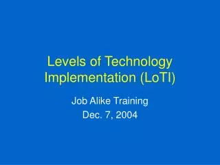
Implementation technology. Transistor Switches. NMOS. PMOS. PMOS. NMOS. PMOS. NMOS Logic Gates. NOT. NAND. NAND. NOR. NOR. CMOS Logic Gates. AND. OR. OR. CMOS NOT. CMOS NAND. CMOS NOR. CMOS AND. 7400. 7400. 74244. Programmable Logic Array.

E N D
3.7 Custom Chips, Standard Cells, and Gate Arrays • The designer of a custom chip has complete flexibility to decide the size of the chip, 1.the number of transistors the chip contains; 2.the placement of each transistor on the chip; 3.the way the transistors are connected together.
layout • The process of defining exactly where on the chip each transistor and wire is situated is called chip layout. • 版面设计、布局布线
Figure 3.42 The logic function in the gate array of Figure 3.41.
3.8 Practical Aspects • robustness of logic circuits逻辑电路的鲁棒性 • signal propagation delays 传输延时 • power dissipation 功耗 • Polysilicon 多晶硅 Extremely small dimensions
MOSFET Fabrication and Behavior • L channel length • W channel width • ON-Resistance 1K • Voltage Level in Logic Gates • Noise Margin 噪声容限
Power Dissipation in Logic Gates • Static Power • Dynamic Power
Fan-in and Fan-out • Fan-in: the number of inputs to the gates • Fan-out: the number of other gates that a specific gate drives
buffer • A logic gate has to drive a large capacitive load • Built with relatively large transistors
Transmission Gates 传输门 • NMOS:passes 0 well and 1 poorly • PMOS :passes 1 well and 0 poorly