Download
1 / 26
260 likes | 461 Views
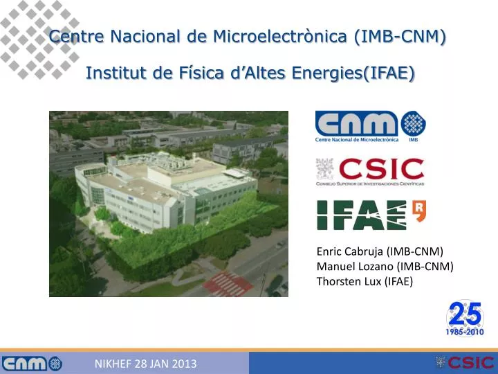
Centre Nacional de Microelectrònica (IMB-CNM). Institut de Física d’Altes Energies(IFAE). Enric Cabruja (IMB-CNM) Manuel Lozano (IMB-CNM) Thorsten Lux (IFAE). Centro Nacional de Microelectrónica. Instituto de Microelectrónica de Barcelona. Project funding splitting:

E N D
Centre Nacional de Microelectrònica (IMB-CNM) Institut de Físicad’Altes Energies(IFAE) EnricCabruja (IMB-CNM) Manuel Lozano (IMB-CNM) Thorsten Lux (IFAE)
Centro Nacional de Microelectrónica Instituto de Microelectrónica de Barcelona Project funding splitting: EU FP: 26 % National (includes Eur. JTI): 40 % Industrial contracts: 35 % 2012 Budget: 11,5 M€ Externalfunding: 49,4 %
R&D ValueChain at CNM product CNM coversalltheValueChain Strategic vs Pragmatic Long term vs short term Top down vs bottom-up Industrial (partic. SMEs) weightbalance in theconsortium idea
IMB-CNM Structure • Micro & NanosystemsDepartment • SystemsIntegrationDepartment • ICTS: Micro & NanointegrationCleanRoom
Integrated Micro and Nano FabricationCleanRoom Main Clean Room • 1,500 m2Class 100-10,000 • CMOS integrated circuits • Microsystems technologies • Nanolithography and nanofabrication Back-end Clean Room • 40 m2 Class 1000 • Chip packaging • High Density FlipChip
Research & ApplicationLaboratories • Microsystems / SensorsCharacterization • General Chemistry/ ChemicalTransducers • BiochemicalSystemscharacterization • ChemicalTransducers • IntegratedOptics • PowerCircuits and Systemscharacterization • Thermalreliability • IntegratedCircuits and systems • Advancedpackaging • RadiationDetectors • Reverse Engineering • IntegratedOptics • SAM/SEM • Prototyping • 3D Rapid Manufacturing
IMB-CNM Research Focus • Energy MICRO & NANO INTEGRATED SYSTEMS • Health • Food and Environment
People 3 permanentdoctors 2 contracteddoctors 4 PhD students 2 Engineer Activitiesstarted in 1996 Experiments Members of the RD50 CERN Collaboration ATLAS, ATLAS upgrade (sLHC) GRI (Gamma RadiationImager) RadiationDetectorsgroup
Silicon radiation detectors Layout design, simulation, fabrication, characterization Pad, strip and pixel designs P-in-N, N-in-P and N-in-N technologies developed Silicon oxigenation 3D detectors Electrodesdeepintosiliconbulk Low full depletionvoltage Pad pitch adaptorsfor detector modules ATLAS-SCT Forward Modules Medical imaging X-rayradiation pixel detectors DEAR-MAMA European Project Real time stereotacticbiopsy Complete pre-industrial system Hardware, software, and chip design Radiationeffectsondevices and materials Thindielectricsforsubmicronictechnologies Siliconradiationdetectors MOS, BiCMOS and bipolar devices High densitybumpbonding Fine pitch byelectrodeposition Forimagedevices Activities in RadiationDetectors
Technologies: P-on-N, N-on-P, N-on-N Pad, strip and pixels detectors High resistivity poly, capacitive coupling, two metal layers, two side processing Limited to 4 inches wafers Radiation hard devices: Oxygenated FZ and magnetic Czochralski silicon. Detector design and fabrication
Sentaurus (Synopsys) Technologysimulation Electricalsimulation Static and dinamic Chargecollection in 3D Detector simulation
DearMama project: digital mammography system Pixel silicon detectors fabricated at CNM We investigated the use of CdTe from Acrorad. Use of Medipix2 chip Detectorsfor x-rayimaging Fabricated at CNM Read-Out at IFAE
In collaboration with IFAE Bump bonding already working Medipix and ATLAS pixels successfully bonded Now working to increase yield and qualify the technology SET/Süss FC150 machine 1 micron placing accuracy In-situ reflow BumpBondingHybridization
1996: start of IFIC-CNM collaboration 1998: first detector fabrication (simple diodes) 1999: silicon oxygenation technology 2000: P-on-N pad detectors (RH 1x1015 cm-2) 2002: P-on-N & N-on-P strip detectors (RH 5x1015 cm-2) 2003: Signature of contract with CERN for pitch adaptors production at CNM clean room for ATLAS End-Cap SCT 2003: N-on-N strip detectors (double-side processing) (RH 5x1015 cm-2) 2005: MCz strip detectors (RH 1x1016 cm-2) 2005: End of ATLAS fanins production at CNM’s Clean Room 2006: Moderated p-spray N-on-P strip detectors 2007: Mammography System 2007: Pixel detectors 2008: 3D detectors technology 2008: ALiBaVa System development 2009: Ultra-thin 3D detectors 2009: Proposal of SiGe tech for FE 2010: Neutron detectors 2010: Edgeless detectors 2010: Evaluation of LDMOS 2011: Transparent detectors for alignment 2011: Signature of contract with CERN for the fabrication of 1/3 IBL of pixel 3D sensors together with FBK Achievements
Pitch adaptor production 10,000 pieces for ATLAS Inner Detector Endcaps in three years The biggest commercial contract of IMB-CNM/D+T WE contracted new technicians working only for this production Good experience Some examples: ATLAS pitch adaptors
Material Silicon doping: n-type Thickness: 800 microns Resistivity: between 20 and 30 kOhm·cm Electrode structures Electrodes formed to run orthogonally on both sides of the silicon. Electrode strip length: ~ 4 cm Electrode strip pitch: 500 µm Electrode strip width: 400 µm Interstrip gap: 100 µm Electrode strip material: End of strip connection suitable for wire bonding. Number of strips: 64 on each side (total 128) Guard ring: Multiple guard ring structures >= 1mm wide with channel stoppers Signal coupling: DC Performance Leakage current < 12 nA/cm2 at 20°C Gettering process to reduce leakage current: Yes Samples delivered D+T will process at least 10 wafers to ensure at least 7 working detectors. The detectors will be delivered cut. Some examples: Double Side Detectors
Double sided 3D technology developed at CNM-Barcelona Holes are etched from both sides Reduction of stress Simplification of fabrication process Not compatible with thin wafers Support wafer ca not be used Complete process at our Clean Room Second demonstration of 3D feasibility after Stanford 3D pixel detectors for Insertable B-layer for ATLAS Current manufacturers: (Stanford+Sintef), FBK, CNM Good results proved with Medipix2 chips Atlas chips under study Some examples: 3D pixel detectors
1) Process backside of thick detector wafer (structured) implant. 2) Bond detector wafer on handle wafer. 3) Thin detector wafer to desired thickness (grinding & etching). 4) Process front side of the detector wafer in a standard (single sided) process line. 5) Etch handle wafer. If necessary: add Al-contacts. Leave frame for stiffening and handling, if wanted Some examples: Thindetectors using SOI wafers
Gas Detector R&D at IFAE T. Lux
T2K: MPGD Detector R&D 2005: Start R&D efforts for a MPGD TPC for T2K European GEM collaboration: UniGe, IFIC, INFN Bari, IFAE • 2 GEM tower • 3 GEM each • ~20x24 cm2 • also small setup at IFAE 21/19 Thorsten Lux (IFAE/UAB)
T2K: MPGD Detector R&D • IFAE participated in setting up testbench • characterization of ~ 90 MM modules • ~12 m2 readout area • nowadays focus on analysis
Electroluminescence Detector R&D • Started for a double beta experiment in 2005 • Set up a high pressure gas system at IFAE • First stage: small chamber with 5 APDs • Allowed to develop readout electronics • Excellent energy resolution achieved • Low threshold possible xenon (8.2 ± 0.1)% FWHM 23
EL Detector R&D • Larger chamber with 25 APDs • Pressure up-to 5 bar • Focus on tracking
Present and Future • GrantedSpanishproject: Openning a new line in gaseousdetectors • Proposalsubmittedto Qatar Foundation: Collaborationwith a group in Qatar?? • Collaborationwithall of you???