Download

1 / 100
1.05k likes | 1.43k Views
Advanced Computer Architecture Memory Hierarchy Design. Course 5MD00 Henk Corporaal November 2013 h.corporaal@tue.nl. Welcome!. This lecture: Memory Hierarchy Design Hierarchy Recap of Caching (App B) Many Cache and Memory Hierarchy Optimizations VM: virtual memory support

E N D
Advanced Computer ArchitectureMemory Hierarchy Design Course 5MD00 HenkCorporaal November 2013 h.corporaal@tue.nl
Welcome! This lecture: • Memory Hierarchy Design • Hierarchy • Recap of Caching (App B) • Many Cache and Memory Hierarchy Optimizations • VM: virtual memory support • AMR Cortex-A8 and Intel Core i7 examples • Material: • Book of Hennessy & Patterson • appendix B + chapter 2: • 2.1-2.6
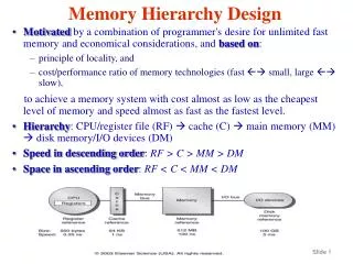
Registers vs. Memory • Arithmetic instructions operands must be registers, — only 32 registers provided (Why?) • Compiler associates variables with registers • Question: what to do about programs with lots of variables ? Fast (2000Mhz) Slower (500Mhz) Slowest (133Mhz) Main Memory 4 Gigabyte CPU Cache Memory 1MB register file 32x4 = 128 byte registerfile
Why does a small cache still work? • LOCALITY • Temporal: you are likely accessing the same address soon again • Spatial: you are likely accessing another address close to the current one in the near future
Memory Hierarchy Design • Memory hierarchy design becomes more crucial with recent multi-core processors: • Aggregate peak bandwidth grows with # cores: • Intel Core i7 can generate two references per core per clock • Four cores and 3.2 GHz clock • 25.6 billion 64-bit data references/second + • 12.8 billion 128-bit instruction references • = 409.6 GB/s! • DRAM bandwidth is only 6% of this (25 GB/s) • Requires: • Multi-port, pipelined caches • Two levels of cache per core • Shared third-level cache on chip
Memory Hierarchy Basics • Note that speculative and multithreaded processors may execute other instructions during a miss • Reduces performance impact of misses
Cache operation Cache / Higher level Memory / Lower level block / line tags data
Direct Mapped Cache • Mapping: address is modulo the number of blocks in the cache
Review: Four Questions for Memory Hierarchy Designers • Q1: Where can a block be placed in the upper level? (Block placement) • Fully Associative, Set Associative, Direct Mapped • Q2: How is a block found if it is in the upper level? (Block identification) • Tag/Block • Q3: Which block should be replaced on a miss? (Block replacement) • Random, FIFO, LRU • Q4: What happens on a write? (Write strategy) • Write Back or Write Through (with Write Buffer)
Direct Mapped Cache Address (bit positions) 3 1 3 0 1 3 1 2 1 1 2 1 0 Q:What kind of locality are we taking advantage of? B y t e o f f s e t 1 0 2 0 H i t D a t a T a g I n d e x I n d e x V a l i d T a g D a t a 0 1 2 1 0 2 1 1 0 2 2 1 0 2 3 2 0 3 2
Direct Mapped Cache • Taking advantage of spatial locality: Address (bit positions)
Cache Basics • cache_size = Nsets x Assoc x Block_size • block_address = Byte_address DIV Block_size in bytes • index = Block_address MOD Nsets • Because the block size and the number of sets are (usually) powers of two, DIV and MOD can be performed efficiently block address block offset tag index 31 … … 2 1 0
6 basic cache optimizations(App. B.3) • Reduces miss rate • Larger block size • Bigger cache • Associative cache (higher associativity) • reduces conflict rate • Reduce miss penalty • Multi-level caches • Give priority to read misses over write misses • Reduce hit time • Avoid address translation during indexing of the cache
Improving Cache Performance T = Ninstr * CPI * Tcycle CPI (with cache) = CPI_base + CPI_cachepenalty CPI_cachepenalty = ............................................. • Reduce the miss penalty • Reduce the miss rate • Reduce the time to hit in the cache
2. Larger Caches • Increase capacity of cache • Disadvantages : • longer hit time (may determine processor cycle time!!) • higher cost • access requires more energy
3. Use / Increase Associativity • Direct mapped caches have lots of conflict misses • Example • suppose a Cache with 128 entries, 4 words/entry • Size is 128 x 16 = 2k Bytes • Many addresses map to the same entry, e.g. • Byte addresses 0-15, 2k - 2k+15, 4k - 4k+15, etc. all map to entry 0 • What if program accesses repeatedly (in a loop) following 3 addresses: (0, 2k+4, and 4k+12) • they will all miss, although only 3 words of the cache are really used !!
Way 3 Set 1 A 4-Way Set-Associative Cache 4-ways: Set contains 4 blocks Fully associative cache contains 1 set, containing all blocks
Example 1: cache calculations • Assume • Cache of 4K blocks • 4 word block size • 32 bit address • Direct mapped (associativity=1) : • 16 bytes per block = 2^4 • 32 bit address : 32-4=28 bits for index and tag • #sets=#blocks/ associativity : log2 of 4K=12 : 12 for index • Total number of tag bits : (28-12)*4K=64 Kbits • 2-way associative • #sets=#blocks/associativity : 2K sets • 1 bit less for indexing, 1 bit more for tag • Tag bits : (28-11) * 2 * 2K=68 Kbits • 4-way associative • #sets=#blocks/associativity : 1K sets • 1 bit less for indexing, 1 bit more for tag • Tag bits : (28-10) * 4 * 1K=72 Kbits
Example 2: cache mapping • 3 caches consisting of 4 one-word blocks: • Cache 1 : fully associative • Cache 2 : two-way set associative • Cache 3 : direct mapped • Suppose followingsequence of block addresses: 0, 8, 0, 6, 8
Example 2: Direct Mapped Coloured = new entry = miss
Example 2: 2-way Set Associative: 2 sets (so all in set/location 0) LEAST RECENTLY USED BLOCK
Classifying Misses: the 3 Cs • The 3 Cs: • Compulsory—First access to a block is always a miss. Also called cold start misses • misses in infinite cache • Capacity—Misses resulting from the finite capacity of the cache • misses in fully associative cache with optimal replacement strategy • Conflict—Misses occurring because several blocks map to the same set. Also called collision misses • remaining misses
3 Cs: Compulsory, Capacity, Conflict In all cases, assume total cache size not changed What happens if we: 1) Change Block Size: Which of 3Cs is obviously affected? compulsory 2) Change Cache Size: Which of 3Cs is obviously affected? capacity misses 3) Introduce higher associativity : Which of 3Cs is obviously affected? conflict misses
3Cs Absolute Miss Rate (SPEC92) Conflict Miss rate per type
3Cs Relative Miss Rate Conflict Miss rate per type
Improving Cache Performance • Reduce the miss penalty • Reduce the miss rate / number of misses • Reduce the time to hit in the cache
4. Second Level Cache (L2) • Most CPUs • have an L1 cache small enough to match the cycle time (reduce the time to hit the cache) • have an L2 cache large enough and with sufficient associativity to capture most memory accesses (reduce miss rate) • L2 Equations, Average Memory Access Time (AMAT): AMAT = Hit TimeL1 + Miss RateL1 x Miss PenaltyL1 Miss PenaltyL1 = Hit TimeL2 + Miss RateL2 x Miss PenaltyL2 AMAT = Hit TimeL1 +Miss RateL1x (Hit TimeL2 +Miss RateL2x MissPenaltyL2) • Definitions: • Local miss rate— misses in this cache divided by the total number of memory accessesto this cache (Miss rateL2) • Global miss rate—misses in this cache divided by the total number of memory accesses generated by the CPU(Miss RateL1 x Miss RateL2)
4. Second Level Cache (L2) • Suppose processor with base CPI of 1.0 • Clock rate of 500 Mhz • Main memory access time : 200 ns • Miss rate per instruction primary cache : 5% What improvement with second cache having 20ns access time, reducing miss rate to memory to 2% ? • Miss penalty : 200 ns/ 2ns per cycle=100 clock cycles • Effective CPI=base CPI+ memory stall per instruction = ? • 1 level cache : total CPI=1+5%*100=6 • 2 level cache : a miss in first level cache is satisfied by second cache or memory • Access second level cache : 20 ns / 2ns per cycle=10 clock cycles • If miss in second cache, then access memory : in 2% of the cases • Total CPI=1+primary stalls per instruction +secondary stalls per instruction • Total CPI=1+5%*10+2%*100=3.5 Machine with L2 cache : 6/3.5=1.7 times faster
4. Second Level Cache • Global cache miss is similar to single cache miss rate of second level cache provided L2 cache is much bigger than L1. • Local cache rate is NOT good measure of secondary caches as it is function of L1 cache. • Global cache miss rate should be used.
5. Read Priority over Write on Miss • Write-through with write buffers can cause RAW data hazards: SW 512(R0),R3 ; Mem[512] = R3 LW R1,1024(R0) ; R1 = Mem[1024] LW R2,512(R0) ; R2 = Mem[512] • Problem: if write buffer used, final LW may read wrong value from memory !! • Solution 1 : Simply wait for write buffer to empty • increases read miss penalty (old MIPS 1000 by 50% ) • Solution 2 : Check write buffer contents before read: if no conflicts, let read continue Map to same cache block
5. Read Priority over Write on Miss What about write-back? • Dirty bit: whenever a write is cached, this bit is set (made a 1) to tell the cache controller "when you decide to re-use this cache line for a different address, you need to write the current contents back to memory” What if read-miss: • Normal: Write dirty block to memory, then do the read • Instead:Copy dirty block to a write buffer, then do the read, then the write • Fewer CPU stalls since restarts as soon as read done
11 Advanced Cache Optimizations (2.2) • Reducing hit time • Small and simple caches • Way prediction • Trace caches • Increasing cache bandwidth • Pipelined caches • Multibanked caches • Nonblocking caches • Reducing Miss Penalty • Critical word first • Merging write buffers • Reducing Miss Rate • Compiler optimizations • Reducing miss penalty or miss rate via parallelism • Hardware prefetching • Compiler prefetching
1. Small and simple first level caches • Critical timing path: • addressing tag memory, then • comparing tags, then • selecting correct set • Direct-mapped caches can overlap tag compare and transmission of data • Lower associativity reduces power because • fewer cache lines are accessed, and • less complex mux to select the right way
Way 3 Set 2 Recap: 4-Way Set-Associative Cache
L1 Size and Associativity Access time vs. size and associativity
L1 Size and Associativity Energy per read vs. size and associativity
Hit Time Miss Penalty Way-Miss Hit Time 2. Fast Hit via Way Prediction • Make set-associative caches faster • Keep extra bits in cache to predict the “way,” or block within the set, of next cache access. • Multiplexor is set early to select desired block, only 1 tag comparison performed • Miss first check other blocks for matches in next clock cycle • Accuracy 85% • Saves also energy • Drawback: CPU pipeline is hard if hit takes 1 or 2 cycles
Way Predicting Instruction Cache (Alpha 21264-like) Jump target 0x4 Jump control Add PC addr inst Primary Instruction Cache way Sequential Way Branch Target Way
BR BR BR 3. Fast (Inst. Cache) Hit via Trace Cache Key Idea: Pack multiple non-contiguous basic blocks into one contiguous trace cache line instruction trace: BR BR BR trace cache line: • Single fetch brings in multiple basic blocks • Trace cache indexed by start address and next n branch predictions
3. Fast Hit times via Trace Cache • Trace cache in Pentium 4 and its successors • Dynamic instr. traces cached (in level 1 cache) • Cache the micro-ops vs. x86 instructions • Decode/translate from x86 to micro-ops on trace cache miss + better utilize long blocks (don’t exit in middle of block, don’t enter at label in middle of block) - complicated address mapping since addresses no longer aligned to power-of-2 multiples of word size - instructions may appear multiple times in multiple dynamic traces due to different branch outcomes
4. Pipelining Cache • Pipeline cache access to improve bandwidth • Examples: • Pentium: 1 cycle • Pentium Pro – Pentium III: 2 cycles • Pentium 4 – Core i7: 4 cycles • Increases branch mis-prediction penalty • Makes it easier to increase associativity
5. Multi-banked Caches • Organize cache as independent banks to support simultaneous access • ARM Cortex-A8 supports 1-4 banks for L2 • Intel i7 supports 4 banks for L1 and 8 banks for L2 • Interleave banks according to block address
5. Multi-banked caches • Banking works best when accesses naturally spread themselves across banks mapping of addresses to banks affects behavior of memory system • Simple mapping that works well is “sequential interleaving” • Spread block addresses sequentially across banks • E.g., with 4 banks, • Bank 0 has all blocks with address%4 = 0; • Bank 1 has all blocks whose address%4 = 1; …
6. Nonblocking Caches • Allow hits before previous misses complete • “Hit under miss” • “Hit under multiple miss” • L2 must support this • In general, processors can hide L1 miss penalty but not L2 miss penalty • Requires OoO processor • Makes cache control much more complex