Download
1 / 18
180 likes | 285 Views
Circuit Modeling of Carbon Nanotubes and Their Performance Estimation in VLSI Design. Arijit Raychowdhury and Kaushik Roy Department of Electrical and Computer Engineering Purdue University, IN. Overview. Introduction to carbon nanotubes and carbon nanotube FETs.

E N D
Circuit Modeling of Carbon Nanotubes and Their Performance Estimation in VLSI Design Arijit Raychowdhury and Kaushik Roy Department of Electrical and Computer Engineering Purdue University, IN
Overview • Introduction to carbon nanotubes and carbon nanotube FETs. • Metallic CNTs as possible interconnect solution. • An RLC model of metallic CNTs. • Simulations and performance predictions. • Metallic CNTs vis-à-vis Cu. • Pros and Cons of CNT interconnects.
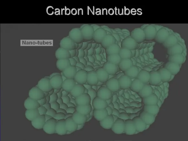
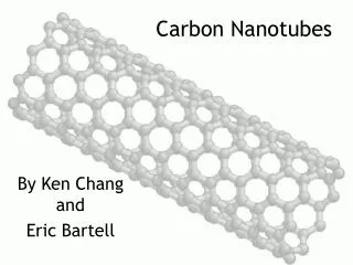
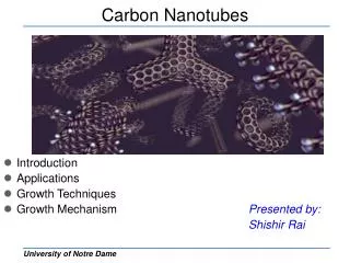
Carbon Nanotubes • Carbon nanotubes are graphite sheets rolled in the form of tubes. • Satisfied C-C bonds • Mechanically strong • Electrically quasi 1D transport close to the ballistic limit Source: IBM
Semiconducting and Metallic CNTs Chirality determines the nature of the CNT • Typical diameters are ~ 0.6nm to 3nm. • The bandgap of semiconducting nanotubes is inversely proportional to the diameter. • The metallic counterparts are studied for interconnects/vias.
Motivation for CNT Interconnects • An all CNT design. • Parasitics will play an important role as the intrinsic gate capacitance is extremely small. • Ultra-small and high reliability. • Cu can handle a max. current density of ~106 A/cm2 whereas CNTs can handle more than 108 A/cm2. • Mechanically strong and no observable electro-migration effects.
R LK CQ CC CQ Modeling CNT Interconnects • RLC Model for CNT Interconnects: • Model the scattering dependant resitance • Incorporates quantum as well as electrostatic capacitances • Models the kinetic (or self) inductance
Nanoscale conduction • Left contact pours in electrons and the right contact drains them out • γis the coupling coefficient Can current increase indefinitely with increasing γ?
Energy Broadening γ The energy level broadens when in contact with a metal. Maximum conductivity for one mode of transport
For V < Vcritical λacc ~ 1.6um V > Vcritical λop ~ 200nm λzo ~ 30nm With Scattering.. For l > the mean free path of phonons
Modeling Resistance Non Linear Resistance Model has been verified with experimental data *Ji-Yong, et. al., cond-mat/0309641, Sept. 28, 2003
r h d Modeling capacitance Electrostatic capacitance due to presence of nearby ground plane. The electrostatic model assumes that the wires are equipotential. But due to the low density-of-states potential drops in the wire ~100 aF/μm vF is the Fermi velocity in graphite ~ 8.1015 m/s
r h Modeling Inductance To add to the magnetic inductance we have kinetic inductance due to finite momentum relaxation time of the electrons (significant for 1D electronic transport) vF is the Fermi velocity in graphite ~ 8.1015 m/s
(m) 1 2 20 Parallel CNTs: Performance estimation Cu at nanoscaled dimensions will have higher resistivity due to grain boundary and surface scattering
z y x N 2 1 2 20 Stacking in the third dimension • The height of Cu is such that JMAX ~ 106 A.cm-2 • We require 200 layers of nanotubes to match the RLC delay of Cu.
Observations • Digital circuits are (most often) voltage driven. • High current density will not reduce the high RLC delay. • Longer interconnects suffer severely from scattering. Even for the smaller ones resistance per nanotube ~ 6KΩ. • Higher frequencies are impeded by kinetic inductance.
Summary • CNTs are highly reliable, can endure two-orders of higher current density than Cu. • Can only be used in relatively slower circuits or in subthreshold operation where the device resistances are high. • CNT interconnects are severely limited by the contact resistances and kinetic inductance. • High current densities do not result in high performance. • Can only be used in relatively slower circuits where the device resistances are high.