Thermoreflectance microscopy and spectroscopy on integrated circuits
170 likes | 351 Views
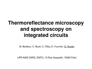
Thermoreflectance microscopy and spectroscopy on integrated circuits. M. Bardoux, C. Boué, C. Filloy, D. Fournier, G. Tessier UPR A005 CNRS, ESPCI, 10 Rue Vauquelin, 75005 Paris. 1 Thermoreflectance under visible illumination. CCD thermoreflectance imaging. 4f < 40 Hz. D R= D T. CCD.

Thermoreflectance microscopy and spectroscopy on integrated circuits
E N D
Presentation Transcript
Thermoreflectance microscopy and spectroscopy on integrated circuits M. Bardoux, C. Boué, C. Filloy, D. Fournier, G. Tessier UPR A005 CNRS, ESPCI, 10 Rue Vauquelin, 75005 Paris
CCD thermoreflectance imaging 4f < 40 Hz DR= DT CCD White lamp Optical measurement of DR (at virtually any wavelength) Filter measurement of DT Microscope Pow.1: f Circuit
FoR j FoDR FoRamb I1 I2 I3 I4 t I1 I2 I3 I4 CCD thermoreflectance imaging 4f < 40 Hz CCD White lamp Filter DR around 10-5 DT around 0.1 K Resolution 300 nm Microscope Amplitude Pow.1: f Circuit
Transistor arrays (ST Microelectronics) Not leaky structures: leaky structures: 13 mm 125 mm 125 mm IDS = 0 - 60 mA, F=1 Hz l=518 nm
Vertical Cavity Surface Emission Lasers (VCSELs) M Bardoux, ESPCI, S. Bouchoule, A. Bousseksou, LPN Laser emission (1.5 mm) VCSEL Cleavage Vertical temperature distribution
Side view (substrate, mirror, active layers) Top view (emission facet) T (°C) Active layers Bragg mirror Substrate 90 mm 250 mm T (°C)
T(K) 80 mm Numerical circuit 180 nm technology (TIMA Grenoble) • Clock frequency 225 MHz • Lock-in at the repetition frequency of the test vectors (7.5 Hz) Thermoreflectance Resolution : 350 nm Backside imaging ?
Thermoreflectance with an InGaAs camera Si Transparency region 4f < 40 Hz InGaAs CCD White lamp Microscope Non coherent sources eliminate interference in the substrate Pow.1: f
Near Infrared back side imaging DR/R X50, 0.6N.A. objective Resolution 2 mm (Diffraction limit : 1.7 mm) Dissipated power : 500 mW
DR/R Resolution difficult to assess (noisy image) Average of FWHM : 650 nm Effective N.A. : 1.55 Diffraction limit with a 0.42 N.A. objective: 2.4 mm
Thermo-/photo- reflectance spectroscopy Compact fibered spectrometer + focusing lens R and vary sharply due to interference CCD spectrometer Spatial selectivity : a few mm Spectral resolution : 1 nm typ. Sensitivity : DR/R~ 3.10-5 in 1 min White Lamp Filter P. Supply 2: 4F Microscope P. Supply 1: F Circuit
Photoreflectance spectroscopy on passive materials SiO2 (glass) Amplitude DR/R Measurement l=615 nm F=0.5 Hz Heating l=10.6 mm F=1 Hz CCD spectrometer White Lamp F=3Hz Filter P. Supply 2: 4F Microscope P. Supply 1: F Modulated CO2 laser F=7.5 Hz Sample 1850 mm
Gold nanospheres in silica (preliminary results) M. Rashidi, B. Palpant, INSP x10-4 DR/R SiO2 + gold nanospheres (≈ 4 nm) Measurement DT ≈ 3 K t= 68 nm Heating l=10.6 mm Si substrate x10-3 DR/R Model DT=50 K Majid Rashidi, INSP
Conclusions 1 ) Visible thermoreflectance resolution ≈ 300 nm precision of calibrated measurement ≈ 5% 2 ) NIR imaging with Solid Immersion Lenses - Resolution : 650 nm at l=1.65 nm, effective N.A.: 1.55 - Resolution improvement : use narrow band illumination better contact SIL / substrate 3) Spectroscopy Fast and sensitive DR/R~ 3.10-5 in 1 min Good spectral resolution (1 nm) Performance spectrometer dependent DR/R~ 5.10-7 should be achievable in 1 min with a 1.5 108 e- well depth.