Download
1 / 40
420 likes | 690 Views
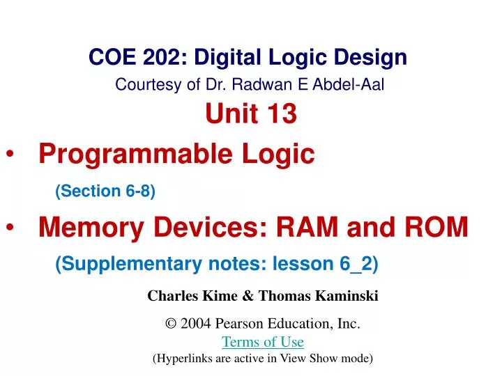
COE 202: Digital Logic Design Courtesy of Dr. Radwan E Abdel-Aal. Unit 13 Programmable Logic (Section 6-8) Memory Devices: RAM and ROM (Supplementary notes: lesson 6_2). Programmable Implementation Technologies: Overview. Why programmable logic?

E N D
COE 202: Digital Logic Design Courtesy of Dr. Radwan E Abdel-Aal Unit 13 • Programmable Logic • (Section 6-8) • Memory Devices: RAM and ROM • (Supplementary notes: lesson 6_2)
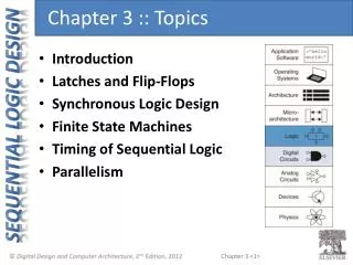
Programmable Implementation Technologies: Overview • Why programmable logic? • Programmable logic techniques and technologies • Programmable Logic Devices: • Read-Only Memory (ROM) • Programmable Array Logic (PAL) • Programmable Logic Array (PLA) • VLSI Programmable Logic Devices (Field Programmable Gate Arrays- FPGA)
Why Programmable Logic? • Facts: • It is most economical to produce an IC in large volumes • But: • Many situations require only small volumes of ICs • Many situations require changes to be done in the field, e.g. Firmware of a product under development • A programmable logic device can be: • Produced in large volumes • Programmed to implement many different low-volume designs
Programmable Logic - Additional Advantages • Many programmable logic devices arefield-programmable, i. e., can be programmed in the field by the user - outside of the manufacturer’s environment • Nowadays, most programmable logic devices are erasable and reprogrammable(i.e. can programmed many times) • Allows “updating” a device or firmware, correction of errors • Allows reuse the device for a different design - re-usability! Concept of Logic Programming Locations of connections determine the logic function implemented
Hardware Programming Technologies • In the Factory - Cannot be erased/reprogrammed by user • Mask programming (changing the VLSI mask) during manufacturing • Programmable only once • Fuse • Anti-fuse • Reprogrammable (Erased & Programmed many times) • Volatile - Programming lost if chip power lost • Single-bit storage element • Non-Volatile - Programming survives power loss • UV Erasable • Electrically Erasable • Flash (as in Flash Memory)
Programmable Logic Configurations:All use AND-OR structure- differ in which is programmable • Programmable Read Only Memory (PROM) - fixed array of AND gates and a programmable array of OR gates • Programmable Array Logic (PAL) - programmable array of AND gates feeding a fixed array of OR gates. • Programmable Logic Array (PLA) - programmable array of AND gates feeding a programmable array of OR gates. How many Possibilities? Fixed or Programmable Connections Fixed or Programmable Connections
ROM, PAL and PLA Configurations Fixed Programmable Fixed Programmable Inputs Outputs AND array Connections Connections OR array (decoder) PROM (a) Programmable read-only memory (PROM) Programmable Fixed Programmable Fixed Inputs Outputs Connections Connections AND array OR array PAL (b) Programmable array logic (PAL) device Programmable Programmable Programmable Programmable Outputs Inputs Connections Connections AND array OR array PLA (c) Programmable logic array (PLA) device
Wiring Conventions for Programmable Logic • We deal with a large number of gates and gate inputs • Need a more concise way of expressing gate circuits • graphically Inputs (literals) A B A B X X 1 wire Inputs X marks a connection, i.e. an input to the OR Output = ?
Read Only Memory (ROM) • Data stored in a ROM is non-volatile • i.e. Once written, this data is permanently stored until erased or changed through re-programming (if applicable) • The ROM has n input lines for the address and m output data lines • So, Total memory capacity of a ROM is 2n x m bits • ROMs do not have input lines as a write operation does not exist in them • Programmable ROMs receive data to be programmed on the output lines • Generally, system-level programs that need to be accessed frequently and at power up access are stored in the computer’s ROM, e.g. the BIOS firmware
1. Read Only Memory (ROM)Programmable sum of (fixed) minterms X X X D0 D1 X X D2 X D3 D4 A2 A X D5 X X B A1 D6 X A0 D7 C F0 F2 F1 F3 • Example: 8 X 4 PROM (n = 3 input lines, m = 4 output lines) • The fixed "AND" array is a“decoder” with 3 inputs and 8outputs implementing minterms • The programmable "OR“array uses a single line torepresent all inputs to anOR gate. An “X” in thearray corresponds to attaching theminterm to the OR • Read Example: For input (A2,A1,A0)= 010, output is (F3,F2,F1,F0 ) = 1001. • What are functions F3, F2 , F1 and F0 in terms of (A2, A1, A0)? 8 X 3-input fixed ANDs give all 8 minterms m0 8 Minterms LSB m7 n I/Ps m O/Ps 2n x m Programmable Connections
Read Only Memory (ROM): n i/ps to m o/ps 2n locations x m bits each • Read Only Memories (ROM) have: • n input (address) lines 2n locations 2n decoded minterms • m output lines (word width) • Fixed array of 2n AND gates implementing all the N-literal minterms. • Programmable OR Array with m outputs lines to form up to m expressions, each being a sum of selected minterm. • The program for a PROM is simply the multiple-output truth table to be implemented • If a 1 entry, a connection is made to the corresponding minterm for the corresponding output • If a 0, no connection is made • Can be viewed as a memory with the inputs as addresses of data (output values), hence ROM or PROM names!Device on previous slide is an 8 x 4 memory (8 locations, each 4 bits) • Truth table is a listing of the memory contents
Read Only Memory (ROM) Advantages/Limitations • Advantages: • Can implement any function (all the minterms are available) • Program is derived directly from the truth table (uses the canonical form) • Disadvantages: • Becomes complex for a large number of inputs n (# of ANDs = 2n, each n-input wide) • Does not support multi-level circuits (no outputs brought back as inputs)
Types of ROM Devices • Simply ROM: Programmed only once and by the manufacturer (in factory), based on the client’s truth table • PROM: A ROM programmable only once by the user (in the field). The user blows fuses to remove unwanted connections. This process is irreversible and hence device is programmed only once • EPROM: Erasable, Programmable ROMs. Can have their data erased using Ultraviolet light and reprogrammed. The user can then reprogram the ROM many times using special programmers Off- situ. Off-situ: Remove from computer to erase/program An EPROM
Types of ROM, Contd. • EEPROMs: Electrically Erasable Programmable ROMs. Have memory cells that can be erased and reprogrammed by exposure to electrical signals. Erasure/Programming is now much easier and in-situ. The processor can now “write” into the EEPROM. • Flash memory devices: • Memory cells are erased in blocks not one-by-one as in EEPROMs Shorter life but faster operation
Read Only Memory (ROM) Naming Conventions determined by Programming Technology
ROM-based Designs • Combinational Circuits: ROMs can be used to implement combinational circuits from their truth tables (i.e. SOm form, without the need for minimization to SOP) • Sequential Circuits: Use ROMs to design the combinational part of the sequential circuit
ROM-based Designs:Combinational Circuits Example 1: Implement the following two combinational functions using a ROM F1 (X,Y) = ∑ m (1,2,3) F2 (X,Y) = ∑ m (0,2) Solution: • Specifying the ROM required: ROM has n = 2 inputs ( 22 = 4 locations) and m = 2 outputs ( Each location has 2 bits) … 4 x 2 bit ROM • Specifying the ROM data content (to be programmed into the ROM): Directly from the truth table of the two functions Index 0 1 2 3
ROM-based Designs:Combinational Circuits Example 2: X2 look-up table, X is 3-bit binary number Specification: Use a ROM to implement a combinational circuit that accepts a 3-bit binary number at the input and generates its square at the output. • Formulation: 8 x 6 bits ROM, Truth Table Observations on the truth table: 1. Output B0 = Input A0 2. Output B1 = Always 0 No need to ‘store’ data for B0 and B1 This reduces the size of the ROM required from 8 x 6 bits to 8 x 4 bits 8 Locations 6 bits
ROM-based Designs:Combinational Circuits Example 2, Continued Truth Table for Reduced ROM Implementations of the X2 Look-up Table: 8 Locations 4 bits
ROM-based Designs:Sequential Circuits : Conventional Design Individual FFs ROM-Register Based Design
ROM-based Designs:Sequential Circuits : Example: Design a sequential circuit that has the following State Transition Table Using a ROM and a Register Q1+ = Σm (1, 2, 5, 6) Q2+ = Σm (4, 6) Y (Q1, Q2, X) = Σm (3, 7) 8 Locations ROM Outputs (Data) ROM inputs (Address) 3 bits 3 bits
ROM-based Designs:Sequential Circuits : The ROM Required Organization Truth Table
ROM-based Designs:Sequential Circuits : Implementation
2. Programmable Array Logic (PAL)Sum of a fixed number of products Product term I A 1 I B 2 B A A C C Programmable AND gates inputs • 4-input, 4-output PAL with fixed, 3-input OR terms • What are the equations for F1 through F4? F1 = + F2 = B + AC + AB F3 = F4 = What if a function uses more than 3 products? Implement as multi-level 0 1 2 3 4 5 6 7 8 9 Fixed X 1 X F X 2 1 3 O/P made available as I/P support multilevel circuits X X X 4 X X F 5 2 X X 6 X X 7 F X X 8 3 X 9 I C 3 X X 10 X X F 11 4 X 12 I 4 0 1 2 3 4 5 6 7 8 9
Programmable Array Logic (PAL) • PAL is the opposite of the ROM, having a set of programmable ANDs combined with a set of fixed ORs- Here programmable means selectable I/Ps • Advantages • For given internal complexity, a PAL can support larger N and M than a PROM • PAL has outputs from OR terms fed as internal inputs to all AND terms, allowing implementation of multi-level circuits • Some PALs have outputs that can be complemented, allowing expressions in terms of a POS: F = F • Disadvantages • Has only a limited number of products (= # of ANDs = # of inputs to an OR). If function needs more product terms it can not be implemented directly in 2-level logic SOP
Programmable Array Logic (PAL), Contd. AND gates inputs Product A A B B C C D D W W term 1 2 W 3 X A All fuses intact 4 (always 0) 5 5 F1 6 B 7 8 F2 9 C 10 11 12 Fuse intact X D Fuse blown 1 A A B B C C D D W W Here: Max of 3 products/section • There is no sharing of the AND gates as in the ROM and PLA. i.e. AND gate outputs (product terms) are not available for connecting to all the ORs (Sums) • Design requires fitting functions within the limited number of ANDs per output (i.e. per OR gate) • We start by single function optimization, trying to fit the function into one section (one SOP) • If the number of terms in a function is greater than the number of ANDs per OR gate (products/section), then we use more than one section to implement an output (multilevel) • If several outputs use the same product, this reduces circuit cost
Programmable Array Logic (PAL) Example AND Inputs Pr od uc t A A B C B C term A B C D W Outputs B A B C A C 1 0 0 1 — — W = C 2 1 1 1 — — + ABC 3 — — — — — 4 1 0 0 — — F1 = X = A + B + W 5 0 1 0 — — 6 — — — — 1 7 1 1 — — — F2 = Y = AB + BC +AC — 8 — 1 1 — 9 1 — 1 — — 10 — — — — — 11 — — — — — 12 — — — — — = W • Equations: F1 = A + B + C + ABC F2 = AB + BC + AC • F1 must befactoredsince fourterms (> 3) • Factor outlast twoterms as W PAL Programming Table Take Compl. Remove both connections Take True. Full gate not used. See next slide PAL comes with all Connections made. Connections that are not needed must be removed How many connections are removed for product 1?, for product 3?
Programmable Array Logic Example AND gates inputs Product A A B B C C D D W W term 1 X X X 2 W X X X 3 X A All fuses intact 4 X X X (always 0) 5 X X 5 F1 X 6 B X 7 X 8 F2 X X 9 X X C 10 11 12 Fuse intact X D Fuse blown 1 A A B B C C D D W W For an unused product, Leave all connections intact Why? = Opposite of ROM: ANDs: programmable ORs: not X
3. Programmable Logic Array (PLA)Programming at both the product and the sum levels A B C A B X 1 X X X B C X X 2 X Fuse intact X Fuse blown A C X 3 X X A B X X 4 X X 0 C C B B A A 1 X F 1 F 2 • What are the equations for F1 and F2? • Could the PLA implement the functions without the XOR gates? PLA with 3-inputs, 4 product terms, 2-outputs, + programmable output inversions n inputs (3) k products (4) Programmable Connections, Get expressions for each group for a PLA with: n inputs, k products, m outputs Programming the Output inversions m outputs (2) Express F2 as a SOP and POS
Programmable Logic Array (PLA) • Compared to ROMs and PALs, PLA is the most flexible economical device: having programmable ANDs, programmable ORs, and programmable output inversions • Advantages • PLA can have large numbers of inputs N and outputs M, permitting implementation of optimized functions that are impractical for a ROM (because of the large number of inputs N required) • A PLA has all of its product terms available for connecting to all outputs, overcoming the problem of the limited number of inputs to each PAL OR • Any product can be shared by all output functions (sums) • Some PLAs have outputs that can be complemented, to give F expressions in terms of product of sum (POS) (inverted SOP of F) • Disadvantage • Often the # of product terms limits the application of a PLA. Solution: Use two-level multiple-output optimizationto reduce the number of product terms required, thus fitting it into the PLA.
Using Programmable Logic Array (PLA) A B C X X X 1 X 2 X X X X X Fuse intact Fuse blown 1 X X 3 X X X 4 X X X 0 X C C B A A B 1 X F 1 F 2 • The set of functions to be implemented must fit the available number of product terms • Any product is available for use by any output, so we try to maximizesharing of products among various outputs • The best approach to fitting is multiple-output, two-level optimization • Since output inversion is available, terms can implement either a function or its complement if this reduces the number of products needed and/or increases sharing of products • For small circuits, use K-maps to optimize individual functions and maximize product term sharing including use of output complementing • For larger circuits, CAD software is used to do this optimization Implement F or F to maximize sharing Of products- easy to invert to get F
Programmable Logic Array (PLA) ExampleF1(A,B,C), F2(A,B,C), PLA: (3 inputs, 4 products, 2 outputs with programmable inversion) B B • K-mapspecifications • How can thisbe implementedwith only four products? • Complete the programming table • Choose implementations (F or F) that use the largest # of shared products! • How many products needed if we implement F1 and F2? BC BC 00 01 11 10 00 01 11 10 A A 1 0 1 0 0 1 0 0 0 0 A 1 A 1 1 0 0 0 0 1 1 1 F1 map F2 map C C F A BC + A B C + A B C F AB AC +BC = = + 1 2 F AB + AC + BC + A B C = F AC AB B C = + + 1 2 PLA programming table Outputs SUM (OR) Programming Inputs Product (C) (T) term A B C F F 1 2 1 AB 1 1 1 – 1 Product (AND) Programming 1 AC 2 1 – 1 1 1 1 BC 3 – 1 1 – 1 0 0 0 4 ABC
Programmable Logic Array (PLA)Example, Contd. A B C X X X 1 X 2 X X X X X Fuse intact Fuse blown 1 X X X 3 X X 4 X X X 0 X C C B B A A 1 X F 1 F 2 Good sharing of products! The 4 products AB AC BC But we actually need F1 as an O/P, not F1- So invert F1 With the XOR ABC Give algebraic expressions of F1 and F2 F2 F1 We inclement F1 Using the PLA then invert it , as this is more economical
2. Memory Devices:Introduction • Storage element Memory device for data storage • One flip flop stores a bit • A set of m flip flops make a register that stores m bits • m = 8: Byte, m = 16: Word, m = 32: double words, m = 64: Quad words, etc. • Over the years, Processors have used larger and larger registers to process data: m = 4, 8, 16, 32, 64, 128 bits
Memory Devices • A memory device consists of a set of registers (memory locations) that share a common set of input lines (input bus) and a common set of output lines (output bus) • With Read/Write memory devices we can store (write) into or read from any memory location • We select which location to access by specifying its address on the address bus • We select a specific memory chip and specify a READ or a WRITE operation using control signals (e.g. RD/WR) on the control bus • Time taken for the read data to appear at the device output after specifying the location address is access time (ns) Chip Select A memory device that we can write into and read from is a Read/Write (RAM) device
Capacity of a Memory Device • Storage Capacity: Number of storage locations x width of data in each location • With Address = n bits Number of registers (storage locations) = 2n locations • If each location is m-bit wide then memory capacity is 2n x m bits • Example: n = 10, m = 8 210 x 8 bits 1K Bytes of storage = 1 KB = 8 K bits What is n, m for a 64 K locations, each being 1 Byte?
Basic Types of Memory Devices • Two Basic Types: • Random Access Memory (RAM): Can be Read or written into • Read Only Memory (ROM): Can be read only. Writing requires programming
RAM Memory • The contents of a RAM can be accessed in random order (so is ROM by the way- a misnomer!) • A better name is Read-Write memory: i.e. Can be read or written into • Has both input and output data lines • Time taken to transfer data to or from any register (storage location) is the same regardless of address • This is different from sequential storage e.g. on tape or disc • Data held in a RAM memory is volatile (not permanent) – Disappears when power is removed Will not survive a power down Use ROM for this purpose
Two main types of RAM Memory Write Read • Static Memory (SRAM): Each bit is stored in a latch Once data is written, it remains as long as power is ON More costly, requires a larger number of transistors, lower storage capacity, faster access times • Dynamic memory (DRAM): Each bit is stored as a chage on a capacitor The charge leaks, and data needs to be refreshed to prevent data loss (snag) Simpler circuit, larger storage capacity, lower cost, slower access time
Overview Unit 13 • Programmable Logic • Memory Devices: RAM and ROM