Download
1 / 11
160 likes | 858 Views
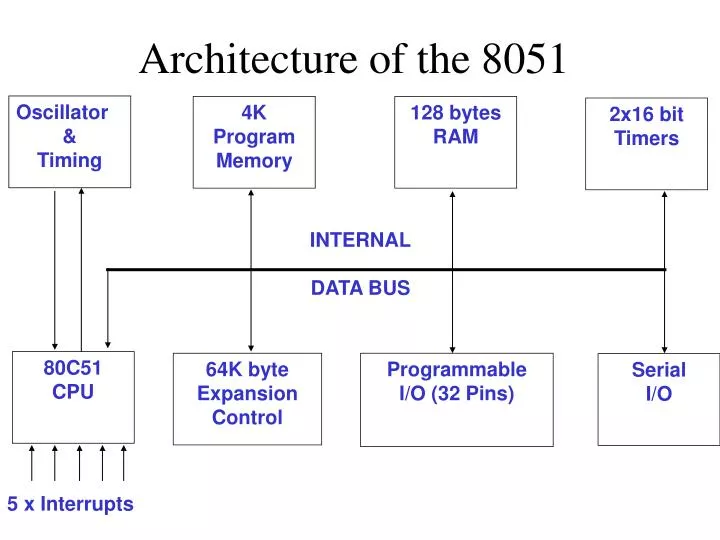
Oscillator & Timing. 4K Program Memory. 128 bytes RAM. 2x16 bit Timers. INTERNAL DATA BUS. 80C51 CPU. 64K byte Expansion Control. Programmable I/O (32 Pins). Serial I/O. 5 x Interrupts. Architecture of the 8051.

E N D
Oscillator & Timing 4K Program Memory 128 bytes RAM 2x16 bit Timers INTERNAL DATA BUS 80C51 CPU 64K byte Expansion Control Programmable I/O (32 Pins) Serial I/O 5 x Interrupts Architecture of the 8051
Oscillator circuit times the CPU: Typical 12 MHz. Note that one machine cycle is 6 states, which are 12 clocks. CPU: Has instruction decoder, ALU, PC and Boolean Processor, Instruction register and interrupt SFRs Interrupt Priority Register (IPR) and Interrupt Enable Register (IEC). 4K PROM: Expandable to 64K using DPTR/PC + MOVX instruction. 128 byte Scratchpad + 128 Addressable bits in the LSByte of SFRs. SFRs include registers A, B, PSW, SP, DPH/DPL 2x16 bit timers: These are controlled with SFRs TMOD and TCON. There is also an interrupt vector for each timer overflow. Expansioncontrol is capable of supporting 64Kbyte of external ROM. 32 I/O pins, pin addressable (some are multiplexed) in 4 x 8 bit port usage. Serial I/O: Two SFRs (SCON, SBUF) are used to control the programmable serial port, which is a full/duplex UART.
1. 8K is 213 so we need 13 address lines. 2. Memory is decoded with '0' active, so we use A13 '0' to CE/. This enables addresses (0000-1FFF) using address lines A0-A12. 3. If A13 goes high addresses (2000-3FFF) become active for the RAM 6164 CS. This CS is active high and therefore only decoded for A13='1' 4. PPI is decoded with A13 active low. It is therefore mutually excluded from RAM but not so with ROM. 5. The PPI is internallydecoded with A1,A2 for programming registers. Potentially there is a problem in that one could read from ROM and think that they are reading a PPI port. To solve this, PSEN/ is only active for ExternalROM access. It can therefore be used with A13 to disable the PPI, as shown above
Timing waveforms for the ROM interface: Note P0 is data/Address multiplexed
ALE: Edge triggered Address Latch Enable. This supports the data address multiplexing. It is used to latch the low PCL address value. ALE Latches addresses A0-A7 from port P0 on the -ve edge. Note that high byte is available directly. • PSEN/: Edge triggered: Progam store enable is a signal that only goes active low during external read cycle. PSEN + ALE control the contents of P0. Address values are needed for external memory access and so PSEN/ needs to combine with ALE. • During the DOWN edge of ALE address low is latched and PCL is on the bus going into ROM. During the next state address is decoded and the next state reads the value at the decoded address. • In the first read it is the instruction. Subsequent reads are again PCL followed by DATA.
POLLING: User controlled, input is strobed by the program at pre-determined intervals. This is useful in slow response systems and convenient because formal proofs are possible and this is especially relevant in time critical systems where formal methods can be used to verify the program. • INTERRUPTS: Program control relinquished to ISR by MAIN upon signal of INT. • Usually vectored, => ISR location is directly available from the INT signal. • Execution and response is never better than 50uS in 8051 family therefore some real time applications can not be supported. • Good for pre-empting and multitasking work however it is virtually impossible to use formal proofs since the point of interrupts can not be predicted. • Interrupts are also prioritised to enable a hierarchical control structure.
1. 5 interrupt sources, each can be individually enabled/disabled.2. Each can be globally enabled/disabled3. Each is vectored to an individual address: Vectoring locates the ISR4. Each can be assigned one of two interrupt levels5. Nesting is possible to two levels6. External interrupts can be level or edge triggered.
Example of a timing routine producing 1ms Pulse: #include <reg51.h>void main(void) ( TMOD=0x01; /* 16-bit timer counter*/TH0=~(1000/256); /* quotient*/TL0=-(1000%256); /* remainder*/TR0=1; /* timer on*/}Counting up to 1000d at 12 Mhz (FFFFh-999d)= FC18hCounting up from FC18 to FFFF will be 999d. A further count up will reset counter to 000 which can be used to signal an interrupt to produce a real time clock.An interrupt occurs every 1 ms in order to allow processor to do other taks ie multitasking.We need to set up the interrupt SFR to signal am interrupt when the counter resets.Intrerrupt 1 is the timer 0 vector at 0BhInterrupt 3 -----||------------------ 1BhThe ISRs have to be located at these vectors
Tutorial exercises: • Q 1. Draw a block diagram of the 8051 micro-controller architecture and explain briefly each component. In your answer, also explain the function of each Special Function Register. Q 2. Draw a diagram showing how an 8031, ROM-less chip can be interfaced to a memory expansion comprising a 16K EPROM and an 8K RAM and also an 8255 Programmable peripheral interface. Also draw the relevant timing waveforms and explain in detail how the full expansion functions. • Q 3. Discuss and contrast the concepts of polling and interrupts in program control for embedded systems. • Q4. Explain in detail the full interrupt structure of the 8051 micro-controller. • Q5. Draw a flow chart and write in C or assembly, a program to provide a real-time clock function by using the timer overflow to signal an interrupt. • (Note: It is not necessary to calculate the frequency of the interrupt)