Download
1 / 8
130 likes | 251 Views
Learn about the internal block diagram, port addressing, data bus, control ports, and different modes of the 8255 programmable peripheral interface chip.

E N D
8255 Programmable Peripheral Interface
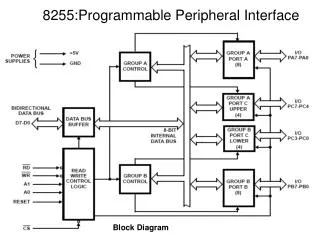
Data bus D[7:0] PA[7:0] A0 8086 PB[7:0] A1 RD Control port WR PC[7:0] RESET A7 CS A6 A5 A4 Port A3 A1 A0 A2 • 0 0 • 0 1 • 0 • 1 1 PA PB PC Control IO/M I/O port address
Different modes Mode 0: Simple Input or Output • Ports A, B, and C can be individually programmed as input or output ports • Port C is divided into two 4-bit ports which are independent from each other Mode 1: Input /Output Control Signals • Ports A and B are programmed as input or output ports • Port C is used for handshaking Mode 2: Bidirectional Data transfer • Port A is programmed to be bi-directional • Port C is for handshaking • Port B can be either input or output in mode 0 or mode 1