Download
1 / 21
210 likes | 322 Views
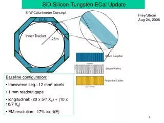
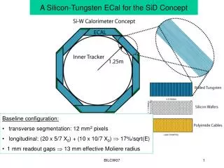
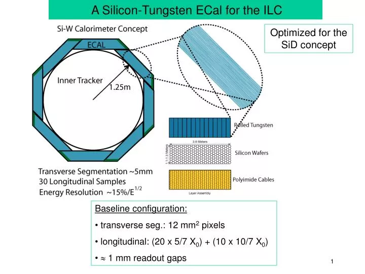
A Silicon-Tungsten ECal for the ILC. Optimized for the SiD concept. Baseline configuration: transverse seg.: 12 mm 2 pixels longitudinal: (20 x 5/7 X 0 ) + (10 x 10/7 X 0 ) 1 mm readout gaps. Silicon detector layout and segmentation. Silicon is easily segmented

E N D
A Silicon-Tungsten ECal for the ILC Optimized for the SiD concept • Baseline configuration: • transverse seg.: 12 mm2 pixels • longitudinal: (20 x 5/7 X0) + (10 x 10/7 X0) • 1 mm readout gaps
Silicon detector layout and segmentation • Silicon is easily segmented • KPiX readout chip is designed for 12 mm2 pixels (1024 pixels for 6 inch wafer) • Cost nearly independent of seg. • Limit on seg. from chip power (2 mm2 ) (KPiX) Fully functional prototype (Hamamatsu)
An “Imaging Calorimeter” A highly segmented ECal is part of the overall detector tracking (charged and neutrals)
Segmentation requirement • In general, we wish to resolve individual photons from jets, tau decays, etc. • The resolving power depends on Moliere radius and segmentation. • We want segmentation significantly smaller than Rm = 10 mm Two EM-shower separability in LEP data with the OPAL Si-W LumCal (David Strom)
Longitudinal Sampling • Compare two tungsten configurations: • 30 layers x 5/7 X0 • (20 x 5/7 X0) + (10 x 10/7 X0) • Resolution is 17% / √E , nearly the same for low energy (photons in jets) • Better for the 20+10 config. at the highest energies (leakage) adopt as baseline
Electronics requirements Use DC-coupled detectors: only two metal layers (cost) • Signals • <2000 e noise • Require MIPs with S/N > 7 • Large dynamic range: Max. signal is 2500 MIPs (for 5mm pixels) • Capacitance • Pixels: 5.7 pF • Traces: ~0.8 pF per pixel crossing • Crosstalk: 0.8 pF/Gain x Cin < 1% • Resistance (traces) • 300 ohm max • Power • If < 40 mW/wafer allows passive cooling (as long as power is cycled off between bunch trains) • Provide fully digitized, zero suppressed outputs of charge and bx time on one ASIC for every wafer.
Beam crossing time structure Since Calor04: Cold ILC chosen Warm • Fast readouts: OK, no pileup • pipeline • bx live: 5 10-3 Cold • Pileup over bunch train • Or fast timing • bx live: 3 10-5 • power pulse
KPiX chip One channel of 1024 Dynamic gain select 12 bit A/D Si pixel Storage until end of train. Pipeline depth presently is 4 Leakage current subtraction Event trigger calibration
Prototype Layout 1x32 1 x 32 Calorimetry 1 x 32 Si Strip Just arrived at SLAC
Tungsten Tungsten ECal schematic cross section New Metallization on detector from KPix to cable Bump Bonds Kapton Data Cable KPix Si Detector Kapton Heat Flow Thermal conduction adhesive Gap 1 mm
“Longitudinal” Data Cable “Transverse” Data Cable Data Concentrator Conceptual Schematic – Not to any scale!!! Locating Pins Readout Chip “KPix” Detectors Tungsten Radiator ~ 1m
Teststand for cosmics, laser and sources • Modified probe station, allows laser to be target on entire detector • IR microscope objective used to focus laser to ~10micron spot • Bias applied to backside of detector using insulated chuck • Use AMPTEK 250F preamp, shapers with ~1 microsec shaping and a digitizing oscilloscope to mockup expected electronics
Response of Detectors to 60KeV Gamma's from Am241 Possible ~1% wafer-wafer calibration?
Noise is consistent with expectation from capacitance and series resistance
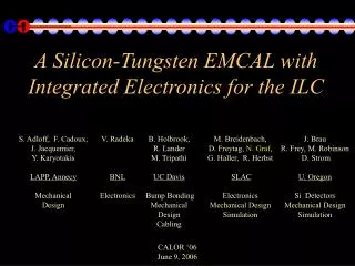
Si/W ECal R&D Collaboration • KPiX readout chip • downstream readout • detector, cable development • mechanical design and integration • detector development • readout electronics • readout electronics • cable development • bump bonding • mechanical design and integration M. Breidenbach, D. Freytag, N. Graf, R. Herbst, G. Haller Stanford Linear Accelerator Center J. Brau, R. Frey, D. Strom, M. Robinson U. Oregon V. Radeka Brookhaven National Lab B. Holbrook, R. Lander, M. Tripathi UC Davis S. Adloff, F. Cadoux, J. Jacquemier, Y.Karyotakis LAPP Annecy