Download
1 / 42
420 likes | 551 Views
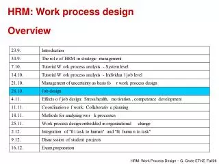
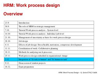
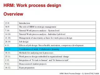
Overview of SoC Design process. References. 1) G. Martin, H. Chang, et al, Surviving the SOC Revolution: A Guide to Platform Based Design, Kluwer Academic Publishers, Sept. 1999.

E N D
References • 1) G. Martin, H. Chang, et al, Surviving the SOC Revolution: A Guide to Platform Based Design, Kluwer Academic Publishers, Sept. 1999. • 2) K. Keutzer, S. Malik, A. R. Newton, J. M. Rabaey, and A. Sangiovanni-Vincentelli, System Level Design: Orthogonalization of Concerns and Platform-Based Design, invited paper, IEEE Transactions on Computer-Aided Design, Vol. 19, No. 12, December 2000.
Four major areas of SoC design(PBD) • Block(IP) authoring • VC delivery • Chip integration • Software development • (Design environment)
Block Authoring • Rapid prototyping; verify the specified functionality based on a combination of real chip versions of IP blocks, emulation of IP in FPGA’s, and optional memory blocks connected to external environment.
Block Authoring • Testbenches; • Quality of TB is a barometer of th e quality of VC. • Stimulus-response, random seed, real-world stream run at all levels from system to transistor level. • Coverage analysis; • RTL linting tools; checks for style and documentation criteria • States, transition arcs, node values, RTL code statements, etc.
Block Authoring • HW/SW coverification; • The purpose is to verify whether the SW is operating correctly in conjunction with HW, i.e., check the handshaking and links between HW register sets and SW. • BFM (bus functional model) suffices for HW, while the SW runs on the model of the target CPU.
Block Authoring • Behavioral simulation; • Based on high-level models with abstracted data representation accurate enough to analyze the architecture and behavior over a range of conditions • BFM or full-functional model (FFM) • Can be cycle-accurate model; correct data changes on each pin at the correct clock cycle and phase • Slower than performance simulation, but generally fast enough to run entire system • Test stimulus and its results can be used as verification suite for design at lower abstraction levels
Block Authoring • RTL(Register-Transfer Level)/Cycle Simulation; • To verify the correctness both in function AND timing. • Models described in RTL (RTL model comprises combinational logic and flip-flops.) which are either cycle-accurate or in more detailed timing. • Cycle-based acceleration possible by assuming all events confined to the rising and/or falling clock edges, ex; Speedsim, VCS of Synopsys • or event-level(driven) simulation ,if the comb. logic delay is modeled ex; VerilogXL, NCVerilog, NCVHDL of Cadence • Relatively slow; typically used to debug critical parts in the circuit. • Testbench can be imported from higher level(function level), and exported to lower level(gate, or logic level) as golden reference.
Block Authoring • Formal Property Checking; • Verify the RTL design against the declared assertions or properties embedded in the HDL code. ex. Assertion-based verification as a compromise bet. formal verification and dynamic simulation • Very efficient( coverage is normally 100%, and verification time is short) • But not always applicable; useful and efficient for limited applications such as • Checking whether the designed interface logic meets bus protocols not falling into lock-up or other failed conditions. • Cache coherence check • State machine
Block Authoring • Analog and Mixed Signal (AMS); • Many analog blocks contains digital circuitry, i.e., they are analog/digital mixed signal hybrids. • AHDL allows mixing analog circuit description into RTL digital blocks for efficient simulation. • Using AHDL (analog HDL) or schematic for analog block is recommended (than layout) for reuse purpose.
Block Authoring • Hierarchical Static Timing/Power Analysis; • STA(Static Timing Analysis); • Evaluate the path delay by adding up delay values of all segments in the path without dynamic simulation • Faster than dynamic simulation • Provided that means for handling state-dependent delays(difference in the path excited and rise/fall delay), off-block loading, clocking schemes(skew and slope) and interface to asynchronous behaviors. • Link to the event simulator required for elements that require dynamic simulation.
Block Authoring • Static Power Analysis(SPA); • Power calculations require a model for the node transition activity extracted, in a probabilistic manner, from a subset of simulation testbench selected hopefully from system-level behavior, if any. • Given the Vdd, clock frequency, GDS II data, the power consumption can be calculated from the model.
Block Authoring • Gate and Mixed-Signal Simulation; • Gate-level digital simulation; • To check whether the timing and functionality(via. RTL testbench) is still satisfied after the synthesis, buffering (repeater insertion), clock tree and I/O cell insertion, DFT(BIST, scan-based testing, and JTAG boundary scan) insertion. • Mixed–signal simulation; • A high-performance device-level simulator, considering the 3-D and layout effects of transistors and interconnects, provides not only functional verification but also timing and power verification.
Block Authoring • Formal equivalence checking; • No testbench necessary • Verifies equivalence between gate-level netlist and structural RTL description • Detected differences (inconsistencies) are reported back to the simulation environment for detailed analysis and debugging
Block Authoring • Physical verification; • Extracts transistor-level connectivity from the layout (GDS II) • Check whether the design rules concerning the layout (DRC) and electrical connectivity (ERC) are met. • Check whether the final design implementation matches the gate-level netlist. • Hierarchical block model helps reduce the verification time.
Block Authoring • Manufacturing test • Virtual System Analysis (assuming designing for reuse purposes); • Identify function, and then performance target (power. speed) and constraints (range of time of usage, range of clock frequency, power consumption, and temperature), external interfaces (I/F standards), target environments. • Similar to the product design with derivatives planning, but requires broader understanding of the target market.
Block Authoring • Constraint budget, obtained as a result of VSD(Virtual System Design); Describes design requirements in terms of • Area • Power • Timing • Test coverage • Time on tester, all in range or discrete values.
Block Authoring • RTL/AHDL specification; • RTL for digital; • RTL into Boolean expression via synthesis, and mapped onto technology-specific library via technology mapping. • RTL writing rules for readability, simulation and synthesis. • AHDL is analog equivalent of HDL and deals with analog equivalent of RTL; • Current status is not good enough for synthesis • Good enough for documentation, and technology migration when provided with schematic of the circuit
Block Authoring • RTL/Logic/Physical Planning; • Planning is THE control point for the physical planning and block implementation. • Planning does 1)assignment of I/O locations for each soft/firm subblock, 2)subblock placement, 3)clock/power/bus tree synthesis and test logic generation, 4)refinement of constraints(power, area, delay, noise budget, etc), 5) accurate prediction of downstream implementation results, 6)management of interconnects through constraints to synthesis, timing, placement and routing.
Block Authoring • Synthesis and custom implementation; • RTL synthesis using cell library and synthesis directives to yield gate-level netlist; clock tree synthesis(CTS) and DFT logic generation; iterated with P&R for closure in timing, IR drop and power consumption. • Synthesis approach is weak when (part of) the design has an internal structure (like datapath which needs another generator/compiler). • Increasing dominance of wires in the overall delay and power budget calls for unified synthesis and P&R, rather than an iteration.
Block Authoring • Clock/Power/Test; • Clock tree/Power net/Test logic insertion typically done during the global routing stage after each placement. • Scan-based testing, BIST with TAP(Test Access Protocol) • Routing; • Begins with constraints from planning & placement in terms of I/O, porosity by layer, clock skew, power buffering, and deals with crosstalk, electromigration. • Routers providing variable line widths, tapering, layer selectivity, understanding the timing model to dynamically react to delay issues are emerging.
Block Authoring • Authoring Guide; • design guide for IP block authors • Specifies outputs of block authoring process, design methodology, requirements of the chip integration process • Includes requirements for documentation, design style, tools, architecture • IP Portfolio; • Set of VC blocks meeting the authoring guide and serving for a limited range of specific applications such as HDTV chip set.
VC Delivery • Formal VC Handoff; • VSI-compliant, self-consistent set of models and data files for the authored block being passed to the chip integrator, so that the design tools and process of both parties(VC producer and VC consumer) have the same semantic understanding of the models. • Protection Methods; • Encryption standards • Watermarking for authenticity proof • Packaging for all views; • Managing and maintaining all versions and changes is crucial for VC delivery, esp. soft VC’s.
Chip Integration • Executable specification; • Chip or product requirements captured and specified in terms of explicit functionality and performance criteria, to be translated into design constraints for the ensuing process • Can be given as simulatable, high-level models with abstract data types and key performance metrics, which can be used for evaluating the appropriateness of the specification itself and testing against the downstream implementation. • Typically given in C, C++, SDL.
Chip Integration • System Analysis; • Develops and verifies the algorithm elements in the design specification • Such developed algorithms are THE base for the fundamental partitioning between HW and SW such that first-order constraints of the specification (application standards, target technology selection) are met.
Chip Integration • VC Selection/Integration • Evaluation of both the blocks available and platform elements for selection • Make modifications (or, refinements) for the available blocks • For new blocks, define the interface requirements and functional behavior.
Chip Integration • Partition/Constraint budget; • HW elements are partitioned and detailed performance, power, area and interface constraints defined for each. • Implementation technology is assessed against each partition and the integration design. • Architectural elements such as power, clock, bus, test, I/O are all put in place. • Initial risk guardband is developed identifying areas where the implementation will need particular attention
Chip Integration • RTL Mapping; The design is mapped into a hierarchical RTL structure, which instantiates VC blocks and selected platform elements(bus, clock, power), and kicks off block design and modification activities.
Chip Integration • Interface Generation; • The interface is manually modified or automatically through parameter change.
Chip Integration • Integration Planning; • Detailed physical planning of the block locations • High-level routing of bus and assembly wiring • Consideration of clock trees, test logic, power controls, analog block locations with noise analysis, and block constraints from overall chip plan.
Chip Integration • Constraint Definition; • Refine the overall constraints based on the floorplan to drive the final layout/route of the integration architecture. • Critical chip-level performance paths and power consumption are analyzed to adjust the constraints based on the interconnect delay and power level extracted from the floor plan.
Chip Integration • Clock/Power/Test; • Generate the clock trees • Lay down power buses and domains considering noise from all different sources (digital-to-analog isolation, ground bounce, simultaneous switching) • Insert test logic
Chip Integration • Hierarchical routing with signal integrity; • Hybrid of high-level assembly and area routing • Considering constraints and signal integrity • Delays and power factors are reported to analysis tools. • Assumptions and assertions made in the VC selection stage are difficult to maintain with VDSM technologies.
Chip Integration • Performance simulation; • Useful for estimating the feasibility of the design goals, or for evaluating different implementation architecture alternatives leading to algorithm selection, architectural choices (HW/SW partitioning tradeoff, VC selection). • Based on high-level models with limited details • ex.) critical path, key functional mode for CPU • Very fast; can be part of system analysis
Chip Integration • Behavioral simulation; • Behavioral models can be either BFM (Bus functional model) for checking interface property only, or FFM (full functional model) for checking internal as well as interface functions. • FFM can be timing-correct (cycle-accurate; signal behavior correct in pin and clock cycle/phase) or not. • Slower than performance simulation, but fast enough.
Chip Integration • Performance simulation; • Useful for estimating the feasibility of the design goals, or for evaluating different implementation architecture alternatives leading to algorithm selection, architectural choices (HW/SW partitioning tradeoff, VC selection). • Based on high-level models with limited details • ex.) critical path, key functional mode for CPU • Very fast; can be part of system analysis
Chip Integration • HW/SW Coverification; • Check whether SW correctly works with HW. • HW is mostly BFM, while SW runs on model of the target CPU (ex; Instruction Set Simulator) • SW can be testbench for the HW
Chip Integration • Rapid Prototyping; • Useful for verifying design elements (HW or SW) in the context of the integration platform architecture and/or with existing VC’s. • Bonded-out core availability counts. • Used for early SW development before the silicon implementation