Download
1 / 21
230 likes | 294 Views
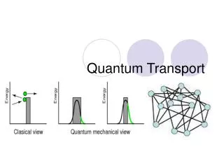
OMEN is a powerful quantum transport modeling tool for nanoelectronic devices, offering 1D-3D simulation capabilities with tight-binding method for accurate results. It enables analysis of various structures and materials, including nanowires and GNR TFETs, optimizing device performance.

E N D
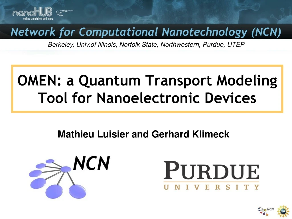
OMEN: a Quantum Transport Modeling Tool for Nanoelectronic Devices Mathieu Luisier and Gerhard Klimeck
http://download.intel.com/technology/silicon/silicon_paper_06.pdfhttp://download.intel.com/technology/silicon/silicon_paper_06.pdf Quantum Dots: Self-assembled , InAs on GaAs. Pyramidal or dome shaped R. Leon et al, JPL (1998) 65nm Node Devices LG=35nm Motivation Why Quantum Transport Simulator? Material variations in 3-D on nm-scale! 45nm Node
OMEN (j) Id-Vgs (l) Electron Density (k) (i) GAA NW • Features: • OMEN: 1D-3D, Parallel, Atomistic, and Full-Band Quantum Transport Simulator (Effective Mass Approx. also Available) From NEMO 1-D to OMENO<-M<-E<-N NEMO 1-D and NEMO 3-D Capabilities => OMEN
OMEN Physical Models Bandstructure Model Nearest-Neighbor pz, sp3, sp3s*, sp3d5s* Tight-Binding Method • GOOD: • bulk CB and VB fitted (BTBT) • extension to nanostructures • atomistic description • BAD: • high computational effort
<r|ψE> = ∑Cij(E,kt)Φσ(r - Rijk)eikt·rt σ σ,ijk,kt What is OMEN? Transport Model 1D/2D/3D Schrödinger Equation H | ψE > = E | ψE > Tight-Binding Ansatz for the Wave Function (E-H-Σ)·GR = I (E-H-Σ)·C = Inj Matrix Inversion Problem Linear System of Eq.
Application to Devices: NW (1) Nanowire Field-Effect Transistors (3D Structures) Simulation of NW FETs: - any channel shape (square, circular, triangular, …) - any transport direction (<100>, <110>, <111>, …) - any gate configuration (gate-all-around, triple-gate, …) - any material (Si, Ge, III-V Compound, …) - n- and p-doped structures - cross section up to 80 nm2, length>100 nm Triple-Gate FET Gate-All-Around FET
Application to Devices: NW (2) Electron –Phonon Scattering in Si Nanowires Gate-All-Around Si Nanowire (d=2.5nm) FET with Scattering Current Reduction : Backscattering and Injection Reduction (ON-Current) Transfer Characteristics Spectral Current
Effective Mass Simulation of III-V HEMTs (1) Experimental Devices: III-V HEMTs for Logic Applications (D.H. Kim et. al, IEDM 07, EDL 08) MIT HEMT: Device Geometry • Objective: • Simulation of III-V Devices (HEMTs) • Challenge the Experiment • Approach: • Real-Space EM Simulations • Realistic Description of Simulation Domain • Injection from Source, Drain, and Gate Contacts • Result: • Match Experimental Results for Various Gate Lengths
Effective Mass Simulation of III-V HEMTs (2) Transfer Characteristics Id-Vgs @ Lg=30, 40, 50 nm All Devices Fitted With One Physical Set of Parameters Lg = 50nm Lg = 30nm Vd=0.5V Vd=0.05V Lg = 40nm Lg = 50nm
Effective Mass Simulation of III-V HEMTs (3) Gate Leakage Current Gate Drain Source Flow Visualization of Gate Leakage Current: Edge Mechanism
GNR TFETs (1) Tunneling Transistor after MOSFET? MOSFET: Thermionic Current TFET: B-to-B Tunn. Current
GNR TFETs (2) Armchair Graphene Nanoribbon • Graphene Nanoribbon: • GOOD: • One-Dimensional Structure • Compatible to Planar Tech. • Low Effective Masses • Tunable Band Gap (Width) • BAD: • Band Gap => Narrow Ribbon • Edges => Roughness Bandstructure of 5.1nm GNR Symmetric CB and VB Band Gap Eg = 0.251 eV
GNR TFETs (3) Structure Definition • TFET p-i-n Structure: • 5.1nm GNR Deposed on SiO2 (N=21) • 1nm EOT (2.35nm Al2O3 with εR=9.1) • 40nm Gate Length • 25nm Source and Drain Extensions • Supply Voltage VDD=0.2 V • Symmetric Doping Conc. • GNR Band Gap Eg=0.251 eV
GNR TFETs (4) Id-Vgs Transfer Characteristics ON-Current: ION=225 μA/μm OFF-Current: IOFF=37 nA/μm Subthreshold Slope SS=12 mV/dec • How can we decrease the OFF-Current? • How can we increase the ON-Current?
GNR TFETs (5) Determination of Supply Voltage • ON-Current Increases with VDD (due to Gate Voltage) • Condition Vbi+VDD<2*Eg must be Satisfied • Condition Broken => Ambipolar Channel Behavior