Download
1 / 27
280 likes | 542 Views
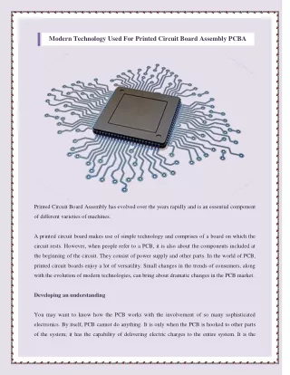
The printed circuit board (PCB) design. PCB design is part of the design process of a product in electronics industry. PCB is a piece of insulating plastic board, on and in which there are several layers of metal (copper) connections that connects parts mounted on the board. .

E N D
The printed circuit board (PCB) design • PCB design is part of the design process of a product in electronics industry. • PCB is a piece of insulating plastic board, on and in which there are several layers of metal (copper) connections that connects parts mounted on the board.
A computer layout of a PCB • The CAD PCB layout consists of several layers. • The electronic components such as resistors, capacitors, ICs and the physical connection between them are usually combined into one diagram in different colors to indicate they are in different layers.
Computer Layout of a PCB A computer layout of a PCB (Cont.)
Distinction between schematic and layout. • The connections on the PCB should be identical to the circuit diagram • The circuit diagram is arranged to be readable, the PCB layout is arranged to be functional
Design flow of PCB • PCB layout can be performed manually (using CAD) or in combination with an Autorouter. • In computer aided PCB design, a typical design flow is as follows:
Design Flow of PCB Design flow of PCB (Cont.)
Design flow of PCB (Cont.) • A designer will enter the design using Schematic Capture does simulation and verification of the functionality of the circuit. • A netlist file is generated by this stage. The netlist is fed into next stage of PCB design which is automatic placement.
Placing Components (Cont.) • First place all the components that need to be in specific locations. • This includes connectors, switches, LEDs, mounting holes, heat sinks or any other item that mounts to an external location. • Give careful of thought when placing component to minimize trace lengths.
Placing Components (Cont.) • Put parts next to each other that connect to each other. • Doing a good job here will make laying the traces much easier. • Arrange ICs in only one or two orientations: up and down, or, right and left.
Placing Components (Cont.) Place the pads for components with fixed or preferred locations on the board.
Orient components so that their packages are parallel with the board’s edges (left), not tilted at random angles (right). Placing Components (Cont.)
Space traces evenly in relation to each other and to pads. Use the shortest routings possible Avoid angles of less than 90 Placing Components (Cont.)
Placing Components (Cont.) • Align each IC so that pin one is in the same place for each orientation, usually on the top or left sides. • Position polarized parts (i.e. diodes, and electrolytic caps) with the positive leads all having the same orientation. • Also use a square pad to mark the positive leads of these components.
Two ways to indicate pin 1 on an IC, using a different-shaped pad (left) or a dot (right). Placing Components (Cont.)
Placing Power and Ground Traces • After the components are placed, the next step is to lay the power and ground traces. • It is essential when working with ICs to have solid power and ground lines, using wide traces (typical 0.025”) that connect to common rails for each supply. • It is very important to avoid snaking or daisy chaining the power lines from part-to-part.
Placing Signal Traces • The standard for layer colors in CAD software is COPPER side (bottom solder layer) is to be RED with the COMPONENT side (top tracked side) to be blue. • When placing traces, it is always a good practice to make them as short and direct as possible. • Use feed-through holes to move signals from one layer to the other. A feed-through holes is a pad with a plated-through hole.
Placing Signal Traces (Cont.) Layer Color
Placing Signal Traces (Cont.) • Generally, the best strategy is to layout a board with vertical traces on one side and horizontal traces on the other. • Add through hole where needed to connect a horizontal trace to a vertical trace on the opposite side.
Placing Signal Traces (Cont.) To route a blocked trace, you can (a) add a jumper (b) move interfacing traces or components or (c) use a double-sided board
For good solder flow onto the pad, traces should be narrower than the pads they connect to. Placing Signal Traces (Cont.)
Placing Signal Traces (Cont.) • It is good idea to place text on the top layer of your board, such as a product or company name. • Text on the top layer can be helpful to insure that there is no confusion as to which layer is which when the board is manufactured.
Placing Signal Traces (Cont.) Route the power supply and ground traces, as well as other critical traces.
Placing Signal Traces (Cont.) Add the short signal traces
Placing Signal Traces (Cont.) Add the long signal traces
Checking Your Work • After all the traces are placed, it is best to double check the routing of every signal to verify that nothing is missing or incorrectly wired.
Checking Your Work (Cont.) • Check for traces that cross each other. This is easily done by inspecting a printout of each layer. • Metal components such as heat sinks, crystals, switches, batteries and connectors can cause shorts if they are place over traces on the top layer. • Inspect for these shorts by placing all the metal components on a printout of the top layer. Then look for traces that run below the metal components.