Download
1 / 3
40 likes | 445 Views
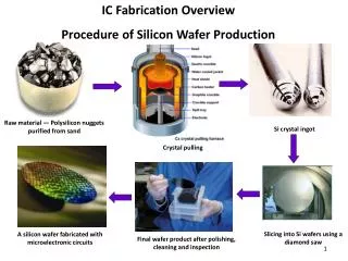
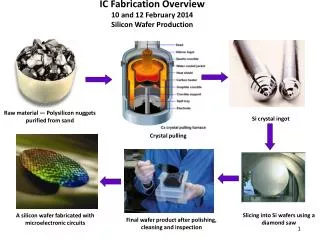
IC Wafer Thinning. Desired thickness goal for front-end ICs on modules is 150 m Prototype results obtained so far have used mechanical thinning(grinding) of bumped wafers. The typical process is Bumps are protected by a layer of photoresist(also useful during dicing)

E N D
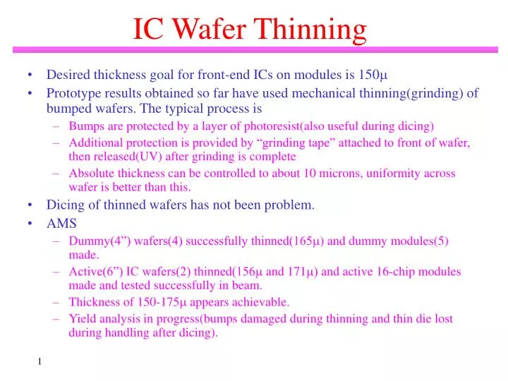
IC Wafer Thinning • Desired thickness goal for front-end ICs on modules is 150m • Prototype results obtained so far have used mechanical thinning(grinding) of bumped wafers. The typical process is • Bumps are protected by a layer of photoresist(also useful during dicing) • Additional protection is provided by “grinding tape” attached to front of wafer, then released(UV) after grinding is complete • Absolute thickness can be controlled to about 10 microns, uniformity across wafer is better than this. • Dicing of thinned wafers has not been problem. • AMS • Dummy(4”) wafers(4) successfully thinned(165m) and dummy modules(5) made. • Active(6”) IC wafers(2) thinned(156m and 171m) and active 16-chip modules made and tested successfully in beam. • Thickness of 150-175m appears achievable. • Yield analysis in progress(bumps damaged during thinning and thin die lost during handling after dicing).
IC Wafer Thinning • IZM • Dummy wafers(6”) have been thinned successfully to 200-210m. Dummy module built, X-rayed and looks OK. • No active wafers thinned yet. • Greater thickness and non-uniformity(edge bead) of photoresist coating limited thickness to about 200m. Breakage, edge chipping below this => use thinner photoresist, and this program has been launched. • Also greater interaction with tape and photoresist - see photos. No bump damage but a concern. Seen also in AMS, but not as much. Reduced by tuning UV exposure, using different tapes but need more experience. • Thickness of 200m demonstrated, plan in place to move towards 150m in next few months. Before photoresist removal After photoresist removal
IC Wafer Thinning • Sofradir • Dummy wafers(4”) thinned to 150mand 200m. • Dummy modules made successfully. • No active wafers thinned yet. • Vendor experience • Thinning of wafers bumped by AMS and IZM done, so far, by Okamoto Corporation in the U.S. This used robotic equipment(except for removal of grinding tape and packaging) and is inexpensive(about 20 chf/wafer(6”) in large quantities). Very large capacity • Thinning of wafers bumped by Sofradir done by MICROPOLISH in France. Cost so far much higher(order of magnitude or more) than Okamoto. • Investigating other vendors. • Have done one wafer using Atmospheric Discharge Plasma technique that is a non-contact method aimed specifically at thin bumped wafers(SmartCard market). Will keep eye on this technique.