Download
1 / 1
10 likes | 109 Views
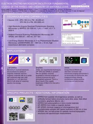
BE3. Increasing Size. Pt 4f UHV. O 1s P = 10 -2 Torr. O 1s P = 100 Torr. Increasing Binding Energy. BE3. BE1. BE2. BE2. Changing Concentration. Intensity. BE1. Alloy Nanoparticle Array. Spectro-microscopy images at various pressures. Decreasing Binding Energy.

E N D
BE3 Increasing Size Pt 4f UHV O 1s P = 10-2 Torr O 1s P = 100 Torr Increasing Binding Energy BE3 BE1 BE2 BE2 Changing Concentration Intensity BE1 Alloy Nanoparticle Array Spectro-microscopy images at various pressures Decreasing Binding Energy ELECTRON SPECTRO-MICROSCOPY FACILITY FOR FUNDAMENTAL STUDIES OF THE PHYSICS AND CHEMISTRY OF MATERIALS (ESM) AP-XPS (k) B. O. Wells et al., Phys. Rev. B 46, 11 830 (1992) ESM Group Leader: E. VescovoProposal Team: D. Arena1, J. Chen 2, T. C. Chiang 3, S. Hulbert1, P.D. Johnson 1, A. Kaminski4, M. Kiskinova5, R. Osgood, Jr.6, R. Reininger1, J. Rodriguez1, J. T. Sadowski1, B. Sinkovic7, K. Smith8, D. Starr1, R. Tromp9, T. Valla1, E. Vescovo1 1Brookhaven National Lab, 2Univ. Of Delaware, 3Univ. Of Illinois, 4AMES Lab, 5ELETTRA, 6Columbia Univ., 7Univ. of Connecticut, 8Boston Univ., 9IBM sample fabrication 10 m High En. ID Low En. ID - + 2 m 200 – 2000 eV 20 – 200 eV aber. corr. PEEM VLS-mono K-Bpair AP-SPEM submeV nano-ARPES TECHNIQUES AND CAPABILITIES • Source: 2 ID – EPU 105 (3 m, PM , 20-200 eV) • EPU 56 (3 m PM, 200-2000 eV) • High-Resolution Angular Resolved Photoemission Scanning Microscopy (m-ARPES): 20-1500 eV, 1 mm, < 1 meV, <0.1o, 5-2000 K • Ambient Pressure Scanning Photoelectron Microscopy (AP-SPEM): 200-1800 eV, < 300 nm, 10+3 Torr • Low-Energy Electron Microscopy & X-ray Photoemission Electron Microscopy (LEEM/XPEEM): 20 – 1800 eV, < 10 nm, high-transmission aberration correction E-range 20 – 2000 eV E-resol. < 1 meV to 70 eV (0.2 meV @ 20 eV) < 10 meV to 1000 eV < 100 meV to 2000 eV Flux >1012 ph/sec @ 10000 resolving power Spot-size 1 mm (K-B), ~ 50 nm (ZP) Applications Comprehensive spectro-microscopy: topography, structure, spectroscopy SPEM in UHV 10m 50 eV m-SP-ARPES: Momentum-resolved electronic structurelectronic bands of magnetic materials and non-magnetic materials with le of solids; spin-polarized arge spin-orbit interaction; a 1 mm spot from NSLS-II will allow for scanning spectro-microscopy. APSPEM: Unites two experimental techniques (AP-XPS and SPEM) to provide < 300 nm spatially resolved, quantitative chemical analysis of surfaces at pressures up to atmospheric pressure. This is a direct result of the superb brightness of NSLS-II in the soft-x-ray region. XPEEM: Energy-filtered XPEEM with aberration-corrected, high transmission imaging spectrometer is an intrinsically non-destructive, fast-imaging technique allowing simultaneous surface-sensitive microscopy and spectroscopy. Specific Projects / ADDITIONAL INFORMATION • ARPES from spatially inhomogeneous samples, as well as artificially formed hetero-structures (nano-dots, wires, field-effect transistors, graphene ribbons, etc.) • ARPES from polycrystalline or micro-crystal materials • SP-ARPES from inside a magnetic domain • AP-SPEM: chemical mapping of inhomogeneous and nanofabricated samples with spatial resolution of 300 nm or less • XPEEM: fast, full-field probe for spatially resolved topographic, structural and spectroscopic measurements ARPES from polycrystals SP-ARPES: topological insulator XPEEM from Fe-nano wires In situ spectro-microscopy of nanoparticle arrays In situ spectro-microscopy of inhomogeneous samples In situ imaging at nanoscale Spatially resolved spectroscopy Ag film on Ni(111) [J. Falta et al.] Organic films