Download
1 / 6
60 likes | 290 Views
EE314 Microprocessor Systems. Chapter 11 Chapter 12. Objectives: The importance of bus buffering How the 8088 addresses (accesses) memory - I/O ports The design of custom memory and I/O address decoders The difference between full and partial address decoding

E N D
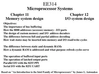
EE314Microprocessor Systems Chapter 11 Chapter 12 Objectives: The importance of bus buffering How the 8088 addresses (accesses) memory - I/O ports The design of custom memory and I/O address decoders The difference between full and partial address decoding How wait states may be inserted into memory and I/O read/write cycles The difference between static and dynamic RAMs How a dynamic RAM is addressed and what purpose refresh cycles serve The operation of buffered input ports The operation of latched output ports Parallel I/O with the 8255 PPI Serial I/O with the 8251 UART Memory system design I/O system design Based on "An Introduction to the Intel Family of Microprocessors" by James L. Antonakos
11.3 Bus Buffering some high Address lines and IO/M used to identify the accessed chip RD WR IO/M A16/S3-A19/S6 A8-A15 8088 AD0-AD7 ALE DEN DT/R READY 74LS244 G1 G2 Memory Address Decoder I/O Address Decoder 8282 STB OE 8282 STB OE D Q LE D Q LE Address Bus WR and RD for each chip 8286 OE T Memory Chip 1 I/O Chip 1 Memory Chip 2 I/O Chip 2 Memory Chip n I/O Chip m Data Bus some low address lines identify the internal accessed byte (more for memory, few for I/O) CE (Chip Enable) or CS (Chip Select), activate each chip the decoder drives READY: provides enough access time for the selected chip
Memory Map - A14 A15 A16 A17 A18 A19 16KB EPROM chip OE A 7 B 6 C 5 74LS138 4 3 E1 2 E2 1 E 0 A0-A13 A0-A13 A19=A18=...=A14=1 select the EPROM CS10 A14 A15 A16 A16, A15, A14 select one EPROM chip 16KB EPROM chip CS9 16KB EPROM chip 16KB EPROM chip 16KB EPROM chip CS8 16KB EPROM chip 16KB EPROM chip 16KB EPROM chip CS7 16KB EPROM chip OE A19 = 1, A18 = 0, A17 = 0 activate the decoder CS6 A17 A18 A19 CS5 220 = 1,048,576 different byte addresses = 1Mbyte CS4 A0 ... A17 CS3 256KB RAM chip MRDC A18 A19 The same Memory-map assignment A0 ... A17 256KB RAM chip WR RD MWTC MRDC A 256Kbyte = 218 RAM chip has 18 address lines, A0 - A17 A18 A19 IO/M A19, A18 assigned to 00 => CS active for every address from 00000 to 3FFFF CS1’ CS1 CS2 A18 = 0 A19 = 0 IO/M = 0 WR RD 8088 Memory Map IO/M = 0 => Memory map All the address lines used by the decoder or memory chip => each byte is uniquely addressed = full address decoding Full address decoding FFFFF FC000 9FFFF 9C000 83FFF 80000 3FFFF 00000 FFFFF FC000 3FFFF 00000 FFFFF 00000 FFFFF FC000 83FFF 80000 3FFFF 00000 FFFFF 3FFFF 00000
Memory Map - A14 A15 A16 A17 A18 16KB EPROM chip OE mirror image A 7 B 6 C 5 74LS138 4 3 E1 2 E2 1 E 0 A0-A13 A0-A13 A18=...=A14=1 select the EPROM mirror image CS10 A14 A15 A16 A16, A15, A14 select one EPROM chip 16KB EPROM chip CS9 16KB EPROM chip 16KB EPROM chip 16KB EPROM chip CS8 16KB EPROM chip 16KB EPROM chip 16KB EPROM chip CS7 16KB EPROM chip OE A19 = 1, A17 = 0 activate the decoder CS6 base image A17 A19 CS5 CS4 A0 ... A15 CS3 base image 64KB RAM chip MRDC A18 A19 The same Memory-map assignment A0 ... A15 64KB RAM chip WR RD MWTC MRDC A 64Kbyte = 216 RAM chip has 16 address lines, A0 - A15 mirror images A18 A19 IO/M A19, A18 assigned to 00 => CS active for every address from 00000 to 3FFFF base image CS1’ CS2 CS1 A18 = 0 A19 = 0 IO/M = 0 WR RD 8088 Memory Map A16, A17 not used => four images for the same chip IO/M = 0 => Memory map Some address lines not used by the decoder or memory chip => mirror images = partial address decoding Partial address decoding FFFFF FC000 DFFFF DC000 CF000 CC000 9FFFF 9C000 83FFF 80000 7FFFF 7C000 3FFFF 30000 2FFFF 20000 1FFFF 10000 0FFFF 00000 FFFFF FC000 9FFFF 9C000 83FFF 80000 7FFFF 7C000 3FFFF 30000 2FFFF 20000 1FFFF 10000 0FFFF 00000 FFFFF FC000 7FFFF 7C000 3FFFF 30000 2FFFF 20000 1FFFF 10000 0FFFF 00000 FFFFF 3FFFF 30000 2FFFF 20000 1FFFF 10000 0FFFF 00000 FFFFF 3FFFF 00000 FFFFF 00000
I/O Map - A2 ... A13 A14 A15 8255 PPI WR RD A0-A1 A15=...=A2=1 select the 8255 chip A 7 B 6 C 5 74LS138 4 3 E1 2 E2 1 E 0 IOWC IORC A2, A1, A0 select one input LATCH (port) CS10 A0 A1 A2 1 byte input port CS9 1 byte input port 1 byte input port 1 byte input port CS8 1 byte input port A15=1,A14...A3= 0 activate the decoder for every address in range 8000...8007 1 byte input port 1 byte input port A14 ... ... A3 CS7 1 byte input port OE CS6 A15 CS5 216 = 65,536 different byte addresses =64Kbyte CS4 CS3 1 byte I/O port WR RD IORC A0 ... ... A15 The same I/O-map assignment 1 byte I/O port WR RD A 1byte I/O port no internal address decoding IOWC IORC A15... A0 assigned to 0 => CS active only for 0000 address A0 ... ... A15 IO/M A0 = 0 ... A15 = 0 IO/M = 1 CS1’ CS1 CS2 WR RD 8088 I/O Map IO/M = 1 => I/O map All A15...A0 used by the decoder or I/O chip => each byte is uniquely addressed = full address decoding Full address decoding FFFF FFFC 8007 ... 8001 8000 0000 FFFF FFFC 0000 FFFF 0000
I/O Map - A2 ... A12 A13 A14 8255 PPI WR RD A0-A1 A14=...=A2=1 select the 8255 chip A 7 B 6 C 5 74LS138 4 3 E1 2 E2 1 E 0 mirror IOWC IORC A3, A2, A1 select one input LATCH (port) CS10 A1 A2 A3 1 byte input port CS9 1 byte input port 1 byte input port 1 byte input port CS8 1 byte input port A15=1,A14...A4= 0 activate the decoder for every address in range 8000...800F 1 byte input port 1 byte input port A14 ... ... A4 CS7 1 byte input port OE CS6 A15 CS5 CS4 base CS3 1 byte I/O port WR RD IORC 216 = 65,536 different byte addresses =64Kbyte A3 ... ... A15 The same I/O-map assignment 1 byte I/O port WR RD A 1byte I/O port no internal address decoding IOWC IORC A15... A3 assigned to 0 => CS active for every address in range 0000 ... 0007 A3 ... ... A15 IO/M A3 = 0 ... A15 = 0 IO/M = 1 CS1’ CS1 CS2 WR RD 8088 I/O Map IO/M = 1 => I/O map Some address lines not used by the decoder or I/O chip => mirror images = partial address decoding Partial address decoding FFFF FFFC 800F mirror 800E base ... 8001 mirror 8000 base 7FFF 7FFC 7 mirrors 0000 base FFFF FFFC 7FFF 7FFC 7 mirrors 0000 base FFFF 7 mirrors 0000 base FFFF 0000