Download
1 / 31
310 likes | 313 Views
Learn how to design and order custom PCBs, from understanding the basics to creating schematic diagrams, placing components, and routing traces.

E N D
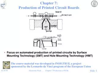
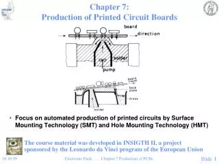
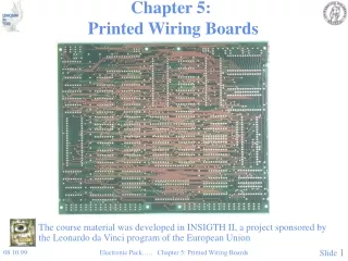
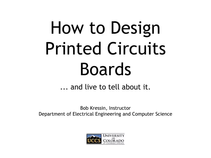
How to Design Printed Circuits Boards • ... and live to tell about it. Bob Kressin, Instructor Department of Electrical Engineering and Computer Science
Overview • What is a Printed Circuit Board? • How do you design a PCB? • How do you order a custom PCB? 2
What is a PCB? A Mechanical Solution to an Electrical Problem Photo from hephaestusaudio.com Photo from www.sparkfun.com 3
What is a PCB? Layers, Traces, Planes, and Vias ... oh my! Image from www.elkosoft.com 4
What is a PCB? Essentially, you’re job is this ... Image from www.gettyimages.com 5
Component Suppliers Where do we get the goods? • For the “weird & wonderful” - • For the “inexpensive everyday” - • For the board itself - www.sparkfun.com www.mouser.com www.4pcb.com
The PCB Design Process From Vision To Reality Schematic Capture Place Components Iteration Route Traces Eagle PCB www.cadsoft.de Generate Gerbers Fab! 7
Eagle PCB A CAD Tool For Designing a Board Control Panel Project Schematic Capture Layout Symbol Footprint Library 8
Eagle PCB Symbol + Footprint + Device = Component Symbol Sym Device Dev Footprint Pac 9
Eagle PCB Stuff I Need To Get Started • A Plan • Block Diagram / Napkin Sketch • Component Selection • Connections and Testing Considerations • Power and Performance Considerations • A New Project • Access to Libraries 10
Eagle PCB It’s all about the planning. Components Connections Power & Performance Passives: 0805, 0603, etc. Mechanical Connections Power Ratings IC Packages: QFN, TQFP, etc. Bus Connections Battery Performance High-Speed / High-Sensitivity Libraries PC Connections 11
Eagle PCB Creating a New Project • Launch Eagle • File -> New -> Project • Enter Project Name • Directory structure taken care of automagically. • Active project is shown with a green light. 12
Eagle PCB Accessing Libraries • Full view of libraries available via Control Panel • Download more from the web and place in the Eagle installation directory in /lbr • Sparkfun has an incredible library of more advanced parts (accelerometers, etc.) • Caution! Just because you see the library in Control Panel doesn’t mean you can access it in your schematic. 13
Schematic Capture Schematic Capture Creating a New Schematic • File -> New -> Schematic • Save it right away. • Don’t worry about creating a Board just yet. • Keep the 100-mil grid. 14
Schematic Capture Schematic Capture Adding Components • Click the Add icon • Find the component in the library • Set values • Don’t see the library? Try Use -> Library 15
Schematic Capture Schematic Capture Adding Global Symbols • Click the Add icon • Find the global symbol in the library (supply1) • Place as if it were a component 16
Schematic Capture Schematic Capture Adding Traces (aka Wires) • Click the Wire icon • Have at it! 17
Schematic Capture Schematic Capture Some General Tips • Avoid changing the grid unless absolutely necessary. • Free Eagle version does not allow “sheets”. • Free Eagle version requires that schematic drives the layout ... not vice-versa. • Groups, Info, and Layers icons are useful. • Pan, zoom, niceties easy to use. • Really care about that “net”? Label it. • Keep it clean - don’t be lazy. • Document! 18
Schematic Capture Place Components Place Components But before you do ... • Passives - 0805 means 0.08” by 0.05” • Connectors - beware of physical fit • Actives - lots of packaging alternatives • Give thought to testability and troubleshooting Thru-Hole (TH) Surface Mount (SMT) DIP LQFP, QFP, TQFP QFN BGA 19
Schematic Capture Place Components Place Components Creating a new board design • From the schematic, choose File -> Switch to Board. • “Create From Schematic”? You bet! • Board window automatically opens. 20
Schematic Capture Place Components Place Components Some Common Tasks • Right-click on top of component, select Move to reposition. • While moving, right-click to Rotate. • Use “Group” wisely. • Right-click to Mirror (change to other side of board) • Use Move to change outline 21
Schematic Capture Place Components Place Components Thinking ahead • Take your time. • Untangle flight lines. • Think about planes. • Consider testability. • Mechanical Fit? • Hard stuff first. • Keep silkscreen. • Think hard about components on 2-sides. 22
Schematic Capture Place Components Place Components Some General Tips • Are your Design Rules setup correctly? • Run the Design Rule Check (DRC) often. • Run the Electrical Rule Check (ERC) often. • Save a snapshot of your placement file. 23
Schematic Capture Route Traces Place Components Route Traces Adding “Waaaahrs” To Your Layout • You want to route, not wire. • You want to ripup, not delete nets. • Are you on the top or the bottom? • Vias are on top and bottom. Easy to add. • DRC often! • Iterate like mad. 24
Schematic Capture Route Traces Place Components Route Traces Some General Tips • Two layers? Have an x-layer and a y-layer. • Don’t forget mounting holes, other nice things. • Add testability features. • Do the “what if?” dance. • Do the cardboard mockup. • Pour Copper. 25
Schematic Capture Generating Gerbers Place Components Route Traces Some General Tips Gen Gerbers Easier than spit! • Using Advanced Circuits? Have I got a script for you ... • This involves the “CAM Processor” ... • Generate critical layers. 26
Schematic Capture Generating Gerbers Place Components Route Traces Sanity Checking The Result Gen Gerbers freedfm.com • You’ll need an account with Advanced Circuits. • Email will be sent confirming design rule checking. • Advanced Circuits even gives you a discount. • Squash any errors, review all warnings. Look for open vias, closed vias, etc. 27
Schematic Capture Generating Gerbers Place Components Route Traces Reviewing The Result Gen Gerbers • ViewMate - Free Gerber Viewer for Microsoft Windows (link on Dr. Wickert’s site). • Review planes, drill holes, and “obvious” defects. Not usually any surprises here. • Biggest error - not exporting the proper layers. 28
Schematic Capture Fab Place Components Route Traces Before you hit “the button” ... Gen Gerbers Fab! • Generate a Parts List (aka “The BOM”) using Export -> Partlist. • Generate a Pin List (aka “The Netlist”) using Export -> Netlist. • Sanity check both. 29
Schematic Capture Fab Place Components Route Traces Some General Tips Gen Gerbers Fab! • Do you have all of your components? Lead time? • Find out what file format your PCB Vendor wants. • Advanced Circuits - GERBER_RS_274X (no, really) • Consider routing it yourself at UCCS. • Consider barebonespcb.com. Really cheap. • Sleep on it. Follow my tradition - 30
The PCB Design Process A Summary of a Lot of Information Schematic Capture Place Components Iteration Route Traces Eagle PCB www.cadsoft.de Generate Gerbers Fab! 31