Download
1 / 13
130 likes | 356 Views
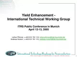
Yield Enhancement - International Technical Working Group ITRS Conference July 18, 2007. Lothar Pfitzner, Fraunhofer-IISB, Erlangen, Germany ++49 9131 761 110, lothar.pfitzner@iisb.fraunhofer.de. Outline. Examples for Yield Loss Chapter Outline Organization of the Chapter

E N D
Yield Enhancement - International Technical Working Group ITRS Conference July 18, 2007 Lothar Pfitzner, Fraunhofer-IISB, Erlangen, Germany ++49 9131 761 110, lothar.pfitzner@iisb.fraunhofer.de
Outline • Examples for Yield Loss • Chapter Outline • Organization of the Chapter • 2007 Key Challenges • Contributors • Subchapters • Defect Detection and Characterization • Wafer Environment Contamination Control • Yield Learning (not active, tables deleted) • Yield Model and Defect Budgets • Outlook
ESD Damage Interconnects overlay Metal 2 crack Via particle open short Metal 1 layer thicknes particle contamination p n p p+ n+ COP interfaces: roughness, state density, charges n-well p-well Si crystal: stacking faults, contamination, stress, COP Examples for Yield Loss • processes: implantation, etching, deposition, planarization, cleaning,… • faults and problems: contamination, particles, defects, overlay faults, OPC, cracks, roughness, stress
bad die good die 300 mm wafer Chapter Outline • Scope and topics • improvement from R&D yield level to mature yield • limited to front-end processing • defect detection and characterization • yield learning/fast ramp Takayuki Ohba, 21 FUJITSU Sci. Tech. J., 38,1,(June 2002): Cross-sectional SEM picture of 10-level Cu dual- Damascene structure fabricated using SiLKTM at the lower level (minimum feature size from M1 to M4) of multilevel interconnects. Gordon Moore: “There is no fundamental obstacle to achieving device yields of 100%.” (Electronics, 38 (8), 1965)
Organization of the Chapter • Chair: Lothar Pfitzner (Fraunhofer IISB) Co-Chair: Dilip Patel (Intel assignee to SEMATECH) • Difficult Challenges • Table YE 2 • Technology Requirements and Potential Solutions • Yield Model and Defect Budget (YMDB) • Chair: Sumio Kuwabara (NEC) - Japan • Table YE 3, YE 4 • Defect Detection and Characterization (DDC) • Chair: Ines Thurner (Qimonda) - Europe • Table YE 5 • Wafer Environment Contamination Control (WECC) – USA • Chair: Kevin Pate (Intel) - USA • Table YE 1, YE 7 • Yield Learning (YL) • Chair: Tings Wang (Promos) - Taiwan • Table YE 6
2007 Key Challenges The Yield Enhancement community is challenged by the following topics: • Near Term (>22 nm) • Detection of Multiple Killer Defect Types / Signal to Noise Ratio –Detection of multiple killer defect types and simultaneous differentiation at high capture rates, low cost of ownership and throughput. It is a challenge to find small but yield relevant defects under a vast amount of nuisance, falsedefects. • Wafer Edge and Bevel Control, Inspection and Review –Defects and process problems around wafer edge and wafer bevel can cause yield problems. • Process Stability vs. Absolute Contamination Level Including the Correlation to Yield data, test structures, and methods are needed for correlating process fluid contamination types and levels to yield and determine required control limits and methods for wafers, optics and masks. • High-Aspect-Ratio Inspection– need for high-speed and cost-effective high aspect ratio inspection tools remains as the work around using e-beam inspection does not at all meet requirement for throughput and low cost. • Linking systematic yield loss to layout attributes - the irregularity of features makes logic areas very sensitive to systematic yield loss mechanisms such as patterning marginalities across the lithographic process window. Solutions exist and need improvements. • Long Term (<22 nm) • In - line Defect Characterization and Analysis –as an alternative to EDX analysis systems. The focus is on light elements, small amount of samples due to particle size and microanalysis • Development of model-based design-manufacturing interface — OPC and considering the high complexity of integration the models must comprehend greater parametric sensitivities, ultra-thin film integrity, impact of circuit design, greater transistor packing, etc.
Europe Ines Thurner (DDC; Qimonda) Lothar Pfitzner (Chair; Fraunhofer IISB) Andreas Nutsch (DDC; Fraunhofer IISB) Andreas Neuber (WECC; M+W Zander) Benoit Hirschberger (DDC; ST) Jan Cavelaars (DDC; Crolles 2/ NXP) Dieter Rathei (DDC/YMDB; DR Yield) Dirk de Vries (DDC/YMDB; Crolles 2/ NXP) Francois Finck (DDC/YMDB; ST) Christoph Hocke (WECC; Infineon) Francesca Illuzzi (WECC; ST) Hubert Winzig (WECC; Infineon) Michael Lurie (WECC; Tower) Michael Otto (WECC; Fraunhofer IISB) Japan Fumio Mizuno (DDC; Meisei Univ. ) Masakazu Ichikawa (DDC; Tokyo Univ.) Isao Kojima (DDC; AIST) Eiichi Kawamura (DDC; Fujitsu) Akira Okamoto (WECC/DDC; Sony) Yoshinori Nagatsuka (DDC; SEIKO-EPSON) Hisaharu Seita (WECC; Sony) Koichi Sakurai (DDC/YMDB; Renesas) Kazuo Nishihagi (WECC; Technos) Ken Tsugane (WECC; Hitachi) Masahiko Ikeno (DB&YM; Hitachi HT) Sumio Kuwabara (DB&YM; NEC EL) Takanori Ozawa (YL/YMDB; Rohm) Yoko Miyazaki (DDC; Accretech ) Yoshimi Shiramizu (WECC; NEC EL) Yuichiro Yamazaki (DDC; Toshiba) Ryu Shioda (YL, Agilent) KatsunobuKitami (WECC, Kurita) Takahiko Hashidzume (DDC, Panasonic) Kazuhiro Honda (DDC; JEOL) Takashi Futatsugi (WECC; Organo) United States (cont.) Dave Roberts (WECC; Air Products) David Blackford (WECC, FMT) Diane Dougherty (WECC) Drew Sinha (WECC, SUMCO) Ed Terrell (WECC; PMS) Frank Flowers (WECC; FMC) James McAndrew (WECC; AirLiquide) Janice Edler (WECC, IBM) Jeff Chapman (WECC; IBM) Jeffrey Hanson (WECC; TI) Jian Wei (WECC; Mykrolis) Jill Card (, Exponent) John Degenova (WECC; TI) John Kurowski (WECC; IBM) Jonathan M. Myers (WECC, IBM) Joseph O’Sullivan (WECC; Intel) Keith Kerwin (WECC; TI) Kosei Matsumoto (WECC, Kurita) Larry Rabellino (WECC, SAES) Luke Lovejoy (WECC; Freescale) Mark Camenzind (WECC; Air Liquide ) Mark Crockett (WECC; Applied Materials ) Rick Udischas (WECC; Ais Liquide) Rob Henderson (WECC; YieldService) Biswanath Roy (WECC; Pall) Sarah Schoen (WECC; Air Liquide ) Slava Libman (WECC; Intel) Scott Anderson (WECC; Air Liquide ) Scott Covington (WECC, Purita) Stephen Toebes (WECC; Brooks) Steve Hues (WECC; Micron Technology) Terry Stange (WECC; Hach Ultra) Tony Schleisman (WECC; Air Liquide ) Tracey Boswell (WECC; Sematech) Val Stradzs (WECC; Intel) William Moore (WECC; IBM) James S. Clarke (DDC; Intel) Kevin Sequin (WECC; Donaldson) 2007 YE ITWG Contributors Korea Uri Cho (; Samsung) Hyun Chul Baek (; Hynix) Sang KyuPark (; Magna Chip) Taiwan Tings Wang (YL; Promos) CS Yang (Winbond) CH Chang (; SIS) ChanYuan Chen (; TSMC) CS Yang (; Winbond) Jim Huang (; UMC) Jimmy Tseng (; PSC ) Len Mei (; Promos Tech ) Steven Ma (; Mxic ) Thank you very much! United States Dilip Patel (Co-chair, DDC, Sematech) Kevin Pate (WECC, Intel) J. Ritchison (DDC; TI) James Dougan (DDC; Freescale) Allyson Hartzell (WECC; Exponent) Aaron Shupp (WECC, PMS) Andrew Bomber (WECC, Intel) Barry Gotlinsky (WECC; Pall) Bart Tillotson (WECC; Fujifilm Electronic Materials) Billy Jones (WECC; Qimonda) Chris Long (WECC; IBM) Chris Muller (WECC; Purafil) Dan Rodier (WECC; PMS) Dan Fuchs (WECC, BOCE) Dan Wilcox (WECC; Spansion)
Defect Budget and Yield Model • 2007 Key Message • Data of defect budget is 6 years old and not applicable to the requirement of introducing Flash in the tables the defect budget table requires an update of PWP data or control limits through IDMs - Requirements: participation by IDMs + budget by IRC • Alternative: delete the defect budget table as it is not state of the art • Enhancement of the defect budget table to give tool suppliers control sizes at measurable defect sizes • 2007 revision • Introduction of Flash as design rule driver • Introduction of material to separate the yield degradation caused by a starting material • Clarification of preconditions for Defect Budgets extrapolation (tableYE 4 and YE 5) • Future objectives • Modeling of systematic mechanism limited yields and description of requirement related to them
Defect Detection and Characterization • 2007 revision • Introduction of flash as design rule driver • Introduction of macro inspection specification • E-beam inspection separated in voltage contrast and physical defect detection • Split of table: • Inspection patterned & HARI • Macro & bevel inspection, unpatterned • Review, Automated Defect Classification • Defect coordinate accuracy for unpatterned inspection tools • Update speed requirements and conditions • future objectives • Bevel review specification • Contamination level of inspection tools
Yield Learning • 2007 revision • proposed to delete the tables due to missing input from IDM • maintain and optimize the text • future objectives • define new outline and support scheme for the sub-chapter
Wafer Contamination and Environment Control 2007 Focus Areas/Revisions • Just clean enough: Revisit specifications, which can be relaxed, if there is not enough process related evidence, why they are needed or why they are at a certain level. • Novel materials: Understand impact of contaminations, which is especially critical since materials change very frequently. Update list of critical ions - New ions to be considered in process monitoring: Pt, Co, Ru, Pd, Hf, La, Zr, Y due to potential cross-contamination issues • Process specific requirements: Continue work to establish process specific requirements • Process integration: Show clearly impact of process integration on specifications, e.g. contamination removal by subsequent cleaning steps, thereby align WECC requirements with FEP, and in the future also Interconnect, Litho and others • Particles as focus item: Continue work on particle specifications and measurement methods and their limitations, especially for small particles down to molecular level, formation and impact of particles.
Wafer Contamination and Environment Control 2007 Focus Areas/Revisions • Impact of Organics (and their species): Which organics are detrimental? Which processes are impacted (e.g. lense hazing)? Is Total Organic Carbon (TOC) a valid parameter vs. individual species? Can we define classes? • Review contaminants in gases: Update gas contaminant lists based on the bulk and specialty gas list similar to ion list • Wafer contamination and environment control (WECC): Complement requirements with environmental process control requirements incl. definition of relevant SPC specification and limits, incl. protection of masks and other critical surfaces such as lenses, another example is the temperature and humidity control specifications for the cleanroom • Supplementary documents: Complement documents about measurement methods and monitoring programs, justification of specifications, process integration examples
Outlook • Development/ Improvement of the Yield Enhancement chapter • Highly active subchapters DDC, WECC, DB&YM improve input to YL or change the focus • Reflection of current activities/future activities requires subsequent adjustment of outline and content of the chapter • Acquire enhanced support for YE Chapter activities (IRC, industrial support, academic inputs, etc.) to ensure that enough and necessary players and resources including academia/supplier participation are present • Request for immediate support and resources to perform urgent required updates (DB&YM)