Download
1 / 24
370 likes | 754 Views
ETCHING. Etching is used extensively in material processing for : delineating patterns, removing surface damage and contamination, and fabricating three-dimensional structures.

E N D
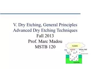
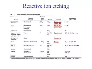
ETCHING • Etching is used extensively in material processing for : delineating patterns, removing surface damage and contamination, and fabricating three-dimensional structures. • Etching is a chemical process whereby material is removed by a chemical reaction between the etchants and the material to be etched. • The etchant may be a chemical solution, in which case the etching process is called wet etching. • The etchant may be a plasma ; plasma-assisted etching is generally referred to as dry etching. The term dry etching (also loosely referred to as plasma etching) is now used to denote several techniques that use plasma in the form of low pressure discharges. • Etching processes are characterized by : • - Etch rate ; material thickness etched per unit time. • - Etch selectivity ; a measure of how effective the etch process is in removing the material to be etched while unaffecting other materials or films present in the wafer. • - Etch uniformity.
Wet Etching • Wet etching involves : (i) transporting the reactants by diffusion to the surface to be etched, (ii) chemical reactions at the surface, and (iii) reaction products transported away from the surface, presumably by diffusion also. • Example : etching of Si in nitric acid/hydrofluoric acid/water • - initially Si is oxidize in the presence of holes: • - water dissociates : • - The hydroxyl ions recombine with positive silicon ions to form silicon dioxide. • - SiO2 dissolves in hydrofluoric acid : • H2SiF6 is soluble in water. • - The overall reaction may be written as :
Directionality In An Etching Process • End-point etch = 0% overetch ; x% overetch corresponds to end-point etch plus an additional etch exposure that would result in etching x% of the thickness of the material to be etched. • Wet etching is "predominantly "isotropic.
Dry Etching (1) Vacuum enclosure ; (2) At least two electrically separated electrodes ; (3) Provision for continuous introduction of etching gas ; (4) A port for pumping ; (5) A source of rf coupled to the electrodes to create plasma.
Mechanisms for Dry Etching e. g., Si Etch by Chlorine Plasma (i) Ion, radical, and electron creation : (ii) Etchant formation : (iii) Adsorption of etchant on substrate : (iv) Reaction to form product : (v) Product adsorption :
Plasma Parameters : Etch-Rate vs Power Frequency Si Etching in Chlorine
Dry Etching : Damage Aspects • Dry etching can be highly directional, however dry etching could be very damaging to etched surfaces and materials.
SEMICONDUCTOR DOPING • Diffusion and ion implantation are the two key processes used to introduce controlled amounts of dopants into semiconductors. • They are used to selectively dope the semiconductor substrate to produce either an n-type or p-type region. • In the diffusion method the dopant atoms are placed on the surface of the semiconductor by deposition from the gas phase of the dopant or by using doped-oxide sources. • In ion implantation method the dopant ions are implanted into the semiconductor by means of a high energy ion beam.
Diffusion • Diffusion of dopants is typically done by placing semiconductor wafers in a furnace and passing an inert gas that contains the desired dopant through it. • The temperatures for doping range between 800 and 1200 °C for Si. • The diffusion process is described in terms of Fick's diffusion equation : • C is the dopant concentration, and D is the diffusion coefficient. • D is expressed as • where Ea is the activation energy for diffusion.
Intrinsic vs Extrinsic Diffusion • The diffusion coefficient is independent of dopant concentration, n, when the doping concentration is less than the intrinsic carrier concentration, ni, at a given temperature. • As n exceeds ni, D becomes dependent on n, and the diffusion process is called extrinsic diffusion.
(I) Infinite-Source Diffusion • It requires a constant surface concentration, CS, of diffusing atoms. • This corresponds to the process step known as “pre-deposition” The initial condition and boundary conditions : The solution to Fick’s equation becomes :
(I) Limited-Source Diffusion • It requires a constant amount of total diffusing atoms per unit area of the diffusing surface ; this is referred to as the dose S. • This corresponds to the process step known as “drive-in”. The initial and boundary conditions are : The solution to Fick’s equation becomes :
Diffusion Profiles Phosphorus in Si (a) Intrinsic diffusion [ the diffusion profile is an error function (erf)]. (b), (c), and (d) are for extrinsic diffusions, and the profiles deviate from erf.
Diffusion-Related Processes : Oxide Masking • The diffusivities of commonly used dopants are considerably smaller in silicon dioxide than in Si. • Hence silicon dioxide can be used as an effective mask against dopants. • Typical diffusivities in the oxide at ~ 900 °C are 3x10-19 cm2/s for B and 10-18 cm2/s for P.
Diffusion-Related Processes : Lateral Diffusion • Diffusion contours obtained by numerical solutions of Fick's two-dimensional diffusion equation. rj is the radius of curvature, x is the depth and y is the lateral dimension.
Ion Implantation : Definition and Equipment • Ion implantation is throwing high energy ions at a substrate. • Commonly implanted elements are B (doping), P (doping), As (doping), O (buried oxide layers), or Si (amorphise polysilicon). • Typical energies ~ 20 to 200 keV, and typical ion densities are 1011 to 16 atoms/cm2 of wafer surface.
Ion Implantation : Ion Distribution Ion distribution is Gaussian
Ion Implantation : Pattern Generation • Ion implantation can be used to do resistless pattern generation : e. g., etch rate enhancement in silicon dioxide when it is implanted with various ions.
Ion Implantation : Modification of Oxidation Rate • After silicon ions are implanted into the silicon substrate, followed by thermal oxidation, the thickness of silicon dioxide increases in the implanted regions.