Download
1 / 21
530 likes | 1.8k Views
Etching. ECE/ChE 4752: Microelectronics Processing Laboratory. Gary S. May February 19, 2004. Outline. Introduction Wet Chemical Etching Plasma Etching. Definition. Recall : Photolithography = process of transferring patterns (on masks) onto a thin layer of photoresist

E N D
Etching ECE/ChE 4752: Microelectronics Processing Laboratory Gary S. May February 19, 2004
Outline • Introduction • Wet Chemical Etching • Plasma Etching
Definition • Recall: Photolithography = process of transferring patterns (on masks) onto a thin layer of photoresist • Photoresist patterns must be transferred once more onto the underlying layers to produce circuit features • Pattern transfer accomplished by selectively etching unmasked portions of a layer
Outline • Introduction • Wet Chemical Etching • Plasma Etching
Uses • Prior to thermal oxidation or epitaxial growth, wafers are chemically cleaned to remove contamination • Especially suitable for blanket etches (i.e., over the whole wafer surface) of polysilicon, oxide, nitride, metals, and III-V compounds.
Mechanism • Reactants transported by diffusion to surface • Reactions occur at surface • Products from surface removed by diffusion
Uniformity • “Equality” of vertical etch rates at different sites on the wafer surface • This is actually non-uniformity • Alternative definitions: s/m
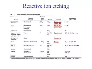
Silicon Etching • Most etchants are mixtures of HNO3 and HF in water or acetic acid (CH3COOH). • HNO3 oxidizes silicon to form an SiO2 layer: Si + 4HNO3 → SiO2 + 2H2O + 4NO2 • HF is used to dissolve the SiO2 layer: SiO2+ 6HF → H2SiF6 +2H2O • Water can be used as a diluent for this etchant, but acetic acid is preferred.
Orientation-Dependent Etching • Some etchants dissolve a certain crystal plane of Si faster than another plane • For Si, the (111) plane has more available bonds per unit area than the (110) and (100) planes • Therefore, etch rate is slower for the (111) plane.
KOH Etching • KOH is an orientation-dependent etchant for Si. • Solution with 19 wt % KOH in deionized water at 80 oC removes the (100) plane at a much higher rate than the (110) and (111) planes [ratio of etch rates for (100):(110):(111) planes = 100:16:1].
SiO2 Etching • Commonly etched in a dilute solution of HF with or without NH4F • Adding NH4F is called a buffered HF solution (BHF), also called buffered-oxide-etch (BOE) • Reaction for SiO2 etching: SiO2+ 6HF → H2SiF6 +2H2O • SiO2 can also be etched in vapor-phase HF.
Outline • Introduction • Wet Chemical Etching • Plasma Etching
Anisotropy • Vertical features are desirable to increase circuit density. • Quantitatively: where RL = lateral etch rate, RV = vertical etch rate
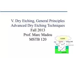
Plasma Fundamentals • Plasma: ionized gas composed of equal numbers of positive and negative charges and a different number of unionized molecules • Produced when electric field is applied to a gas, causing gas to break down and become ionized • Initiated by free electrons that gain kinetic energy from electric field, collide with gas molecules, and lose energy. • Energy transferred causes the gas molecules to be ionized (i.e., to free electrons). • Free electrons gain kinetic energy from the field, and the process continues.
Plasma Etching • Plasma etching - chemical reaction combined with physical ion bombardment • Other names: • ion milling • sputter etching • reactive ion etching • reactive ion beam etching • First explored as a cheaper alternative to wet solvent resist stripping in 1960’s and 70’s
Etch Mechanism • Etchant species generated in plasma. • Reactant transported by diffusion to surface. • Reactant adsorbed on the surface. • Chemical reaction (along with ion bombardment) forms volatile compounds. • Compounds desorbed from surface, diffused into the bulk gas, and pumped out by vacuum system.
End-Point Control • Dry etching has less etch selectivity than wet. • Plasma reactor must be equipped with a monitor that indicates when the etching process is to be terminated (“end point detection” system). • Laser interferometry is used to determine the end point.
Laser Interferometry • Intensity of laser light reflected off thin film surface oscillates. • Period of the oscillation related to change in film thickness where Dd = change in film thickness, l is the wavelength, and is the refractive index
Interferometry Example • Typical signal from a silicide/polycrystalline Si gate etch • Dd for polysilicon = 80 nm (measured by using a He-Ne laser with l = 632.8 nm)