Download
1 / 19
190 likes | 333 Views
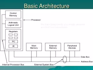
Section II Basic PLD Architecture. Section II Agenda. Basic PLD Architecture XC9500 and XC4000 Hardware Architectures Foundation and Alliance Series Software. Section II Basic PLD Architecture XC9500 and XC4000 Hardware Architectures. 3. In-System Programming Controller. JTAG Controller.

E N D
Section II Agenda • Basic PLD Architecture • XC9500 and XC4000 Hardware Architectures • Foundation and Alliance Series Software
Section IIBasic PLD ArchitectureXC9500 and XC4000 Hardware Architectures
3 In-System Programming Controller JTAG Controller JTAG Port Function Block1 I/O I/O Function Block 2 I/O I/O Blocks FastCONNECT Switch Matrix I/O Function Block 3 Global Clocks 3 Global Set/Reset 1 Function Block 4 Global Tri-States 2 or 4 XC9500 CPLDs • 5 volt in-system programmable (ISP) CPLDs • 5 ns pin-to-pin • 36 to 288 macrocells (6400 gates) • Industry’s best pin-locking architecture • 10,000 program/erase cycles • Complete IEEE 1149.1 JTAG capability
XC9500 - Architectural Features • Uniform, all pins fast, PAL-like architecture • FastCONNECT switch matrix provides 100% routing with 100% utilization • Flexible function block • 36 inputs with 18 outputs • Expandable to 90 product terms per macrocell • Product term and global three-state enables • Product term and global clocks • Product term and global set/reset signals • 3.3V/5V I/O operation • Complete IEEE 1149.1 JTAG interface
Global Clocks Global Tri-State 2 or 4 3 I/O Macrocell 1 Product- Term Allocator AND Array 36 From FastCONNECT I/O Macrocell 18 To FastCONNECT XC9500 Function Block Each function block is like a 36V18 !
XC9500 Product Family 9536 9572 95108 95144 95216 95288 Macrocells 36 72 108 144 216 288 Usable Gates 800 1600 2400 3200 4800 6400 tPD (ns) 5 7.5 7.5 7.5 10 10 Registers 36 72 108 144 216 288 Max I/O 34 72 108 133 166 192 VQ44 PC44 PC44 PC84 TQ100 PQ100 PC84 TQ100 PQ100 PQ160 PQ100 PQ160 Packages HQ208 BG352 PQ160 HQ208 BG352
XC9500XL 3.3V Key Features • High performance • tPD = 4ns, fSYS = 200MHz • 36 to 288 macrocell densities • Lowest price, best value CPLD • Highest programming reliability • 10,000 program/erase cycles • Most complete IEEE 1149.1 JTAG support • Space-efficient packaging, including chip scale pkg • Industry’s first 0.35um Flash CPLD 200MHz 125MHz XC9500XL XC9500
Identical FBs, macrocells and I/Os Maximum Flexibility 54-input function block fan-in 90 p-terms per output 3 global, locally invertible clocks global set/reset pin p-term OE per macrocell clock enable Advanced, 2nd Generation Pin-Locking XC9500XL Embraces In-System Changes
New XC9500XL 3.3V Family XC9536XL XC9572XL XC95144XL XC95288XL 288 Macrocells 36 72 144 6400 Usable Gates 800 1600 3200 tPD (ns) 4 5 5 6 200 178 178 151 fSYSTEM Packages (Max. User I/Os) 44PC (34) 64VQ (36) 48CS (36) 44PC (34) 64VQ(52) 100TQ (72) 48CS (38) 100TQ (81) 144TQ (117) 144CS (117) 144TQ (117) 208PQ (168) 352BG (192) BGA CSP
XC4000 Architecture Programmable Interconnect I/O Blocks (IOBs) Configurable Logic Blocks (CLBs)
C2 C1 C3 C4 H1 DIN S/R EC S/R Control G4 DIN SD G G3 F' Q D Func. G' YQ G2 H' Gen. G1 EC RD 1 H G' Y Func. H' S/R Control Gen. F4 F F3 DIN SD Func. F' F2 Q D XQ Gen. G' F1 H' EC RD 1 H' X F' K XC4000E/X Configurable Logic Blocks • 2 Four-input function generators (Look Up Tables) - 16x1 RAM or Logic function • 2 Registers - Each can be configured as Flip Flop or Latch - Independent clock polarity - Synchronous and asynchronous Set/Reset
A B C D Z 0 0 0 0 0 0 0 0 1 0 0 0 1 0 0 0 0 1 1 1 0 1 0 0 1 0 1 0 1 1 . . . 1 1 0 0 0 1 1 0 1 0 1 1 1 0 0 1 1 1 1 1 Combinatorial Logic A B Z C D WE G4 G G3 Func. G2 Gen. G1 Look Up Tables Look Up Table • Combinatorial Logic is stored in 16x1 SRAM Look Up Tables (LUTs) in a CLB • Example: 4-bit address 4 (2 ) 2 = 64K ! • Capacity is limited by number of inputs, not complexity • Choose to use each function generator as 4 input logic (LUT) or as high speed sync.dual port RAM
XC4000X I/O Block Diagram Shaded areas are not included in XC4000E family.
CLB CLB Switch Matrix Switch Matrix CLB CLB Xilinx FPGA Routing • 1) Fast Direct Interconnect - CLB to CLB • 2) General Purpose Interconnect - Uses switch matrix • 3) Long Lines • Segmented across chip • Global clocks, lowest skew • 2 Tri-states per CLB for busses • Other routing types in CPLDs
Other FPGA Resources • Tri-state buffers for busses (BUFT’s) • Global clock & high speed buffers (BUFG’s) • Wide Decoders (DECODEx) • Internal Oscillator (OSC4) • Global Reset to all Flip-Flops, Latches (STARTUP) • CLB special resources • Fast Carry logic built into CLBs • Synchronous Dual Port RAM • Boundary Scan
Programmable Interconnect Points, PIPs (White) Routed Wires (Blue) What’s Really In that Chip? Switch Matrix Direct Interconnect (Green) CLB (Red) Long Lines (Purple)
XC4000XL Family 4005XL 4010XL 4013XL 4020XL 4028XL Logic Cells 466 950 1,368 1,862 2,432 Typ Gate Range* 3 - 9K 7-20K 10-30K 13-40K 18-50K (Logic + Select-RAM) Max. RAM bits 6K 13K 18K 25K 33K (no Logic) I/O 112 160 192 224 256 Initial Packages PC84 PC84 PQ100 PQ100 PQ160 PQ160 PQ160 PQ160 PQ208 PQ208 PQ208 PQ208 HQ208 PQ240 PQ240 HQ240 BG256 BG256 BG256 BG352 BG352 4036XL 4044XL 4052XL 4062XL 4085XL 40125XV Logic Cells3,0783,800 4,598 5,472 7,448 10,982 Typ Gate Range* 22-65K 27-80K 33-100K 40-130K 55-180K 78-250K (Logic + Select-RAM) Max. RAM bits 42K 51K 62K 74K 100K 158K (no Logic) I/O 288 320 352 384 448 544 Initial packages HQ208 HQ240 HQ240 HQ240 HQ240 BG352 BG432 BG432 BG432 BG432 PG411 PG411 PG411 PG475 PG559 PG559 BG560 BG560 BG560 BG560 * 20-25% of CLBs as RAM * 25-30% of CLBs as RAM
CPLD or FPGA? • FPGA • SRAM reconfiguration • Excellent for computer architecture, DSP, registered designs • ASIC like design flow • Great for first year to graduate work • More common in schools • PROM required for non-volatile operation • CPLD • Non-volatile • JTAG Testing • Wide fan-in • Fast counters, state machines • Combinational Logic • Small student projects, lower level courses • Control Logic