Download
1 / 18
180 likes | 192 Views
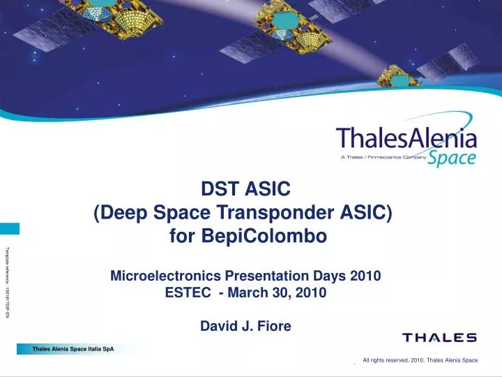
DST ASIC (Deep Space Transponder ASIC) for BepiColombo Microelectronics Presentation Days 2010 ESTEC - March 30, 2010 David J. Fiore. DST ASIC Presentation Overview. DST ASIC Project Overview Overall and specific technical goals SOC design strategies DST ASIC Architecture Overview

E N D
DST ASIC (Deep Space Transponder ASIC) for BepiColomboMicroelectronics Presentation Days 2010 ESTEC - March 30, 2010David J. Fiore
DST ASIC Presentation Overview • DST ASIC Project Overview • Overall and specific technical goals • SOC design strategies • DST ASIC Architecture Overview • DST ASIC general information • DST ASIC block diagram • LEON2-FT Implementation • LEON2-FT Peripheral Implementation • FPGA Prototyping • Project Experiences • Achievements • main problems found • lessons learnt
DST ASIC Overall Technical Goals • The DST ASIC represents the signal processing core of the new generation Deep Space Transponder equipment whose first application will be in the frame of the BepiColombo program. • Operative threshold: down to -150 dBm • Fully configurable telecomm. and telemetry (multi-standard) • Doppler shift up to 1 MHz • Frequency band (up/down): S, X, Ka • Accurate ranging (standard and regenerative): better than 1 m • Coherent and non-coherent operation • Output power: up to +12 dBm BepiColombo Deep Space Transponder (EM) • The design includes all the functions needed for carrier recovery and data demodulation on the receiver side, and advanced design schemes needed to support several modulation formats in order to improve the space-to-earth link performance, on the transmitter side. • The foreseen integration of the LEON2FT Microprocessor (ESA IP) within the DTS ASIC, allows a full programmability and control of the TTC modem in the context of the most advanced space applications and recently issued standards. • The Leon2FT Microprocessor (ESA IP) implements a 32-bit processor conforming to the IEEE-1754 (SPARC V8) architecture.
DST ASIC Specific Technical Goals • The DST ASIC includes a complete set of digital processing functions to cover all TT&C standard (FM, PM, spread-spectrum, deep-space). • Gated clocks (7) for each DSP function (AHB Slaves) are used to reduce power consumption in the different configurations) Demodulated Telecommand LEON2 RT Carrier Demodulator Processor Baseband Processor Command Demodulator Spread- Spectrum Receiver Carrier Modulator Processor TLM Stream’s DST ASIC MUX Spread-Spectrum Ranging Processor DDS Modulator From ADC Standard Receiver (PM/FM) To DAC’s Standard Ranging Processor Ancillary Functions Operational Mode (Standard/Spread-spectrum)
DST ASIC SOC Design Strategies • Keep as much of the ESA LEON2 IP package “as is” (try to utilize the same blocks and same configurations - change as little as possible!). • This is very useful when using the supplied overall testbenches and for debugging in general. (there is a “default” LEON platform to compare results against.) • Blocks that utilize the same clock frequency as the LEON2/AMBA, will be implemented as APB slaves. • Blocks that utilize clock frequencies different than the LEON2/AMBA, will be implemented as AHB slaves. • Utilize the wait states to hold the transaction until re-synchronization is complete. • This re-synchronization is completely decoupled from the AMBA bus and does not involve any hand-shaking – it is completely managed by a circuit using the same clock frequency as the LEON configured with pre-determined number of wait states. • Design a standard AHB AMBA wrapper to be utilized by all designers. This creates a uniform and more manageable design and eliminates the designer from dealing with the AMBA bus. Certain parameters (such as wait states and number of sub-slaves are hard-configurable) • This wrapper divides each AHB slave into 1 to 4 “sub-slaves” to help in organizing design and manage AHB slaves with different functions and different designers. These “sub-slaves” are transparent to the AHB bus. • Certain rules were created for each designer to follow in order to keep overall uniformity and facilitate the overall design flow. • LEON / AMBA clock frequency is 25.6MHz.
DST ASIC General information • ATMEL MH1-332E Gate Array • 0.35 CMOS • Gate Complexity: 1.64 million typical routable gates • MQFPT 352 Ceramic Quad Flat Package • 273 used I/O pins • 78 Power Pins • Operating Conditions • Temperature range for die (°C):-55, +145 • Radiations (dose) : 200 Krads • Power supplies (V%) : 3.3V 10% (Core) 3.3V 10% (I/O) • Max frequency :76.8 MHz • Estimated power : • 5.0 W at 3.3V , load 20 pF and system clock frequency of 76.8 MHz • No internal RAM available in this technology • SEU hardened registers for critical blocks • Scan chain implemented yielding 95% fault coverage • Present status: • Sign-off in April 2010
DST ASIC SOC configuration PROM SRAM I/O (FPGA) add 15 add 19 RS232 data 8 APB used here only for configurataion. data 16 add 19 APB IF AHB Serial Debug Interface UART of AHB Memory Controller (with EDAC) APB IF DSU (Debug Support Unit) LEON2FT integer unit AHB-Interface APB used here only for configurataion. AHB-Interface AHB-Interface AHB-Interface I-cache D-cache APB IF AHB Arbiter/ decoder AHB 32 AHB-Interface AHB-Interface AHB-Interface AHB-Interface AHB-Interface AHB/AHP Bridge DSP slv#3 DSP slv#4 DSP slv #9 1553 Slv #10 … APB 32 APB-Interface APB-Interface APB-Interface APB-Interface APB-Interface APB-Interface APB-Interface APB-Interface APB-Interface UART #1 Timers/ Watchdog GPIO (16bit) Interrupt#1 cntrl Housekeeping MLDS LSSB PLL Peregrine SIPO/PISO APB-Interface APB-Interface APB-Interface APB-Interface UART #2 Interrupt #2 cntrl Scratch Pad (rad-hard) CAN RS232 Legend ESA IP ESA IP Master TAS-I external Other IP ASIC gateclk3 gateclk4 gateclk9 clk12MHz APB-Interface APB-Interface Wr Protect AHB Status
DST ASIC LEON2-FT implementation LEON2-FT implementation: • LEON2-FT version: the newest version of VHDL - LEON2-FT v1.0.9.16.2. • LEON2-FT Cache (both data and instruction) : 1 set, direct mapped. Implemented as a synchronous (register-based) memory and protected by 2 parity bits. This creates a 1 kbyte cache memory organized as 256x34 and a Tag memory organized as: 32x32. • LEON2-FT Register File : 8 windows. Implemented as a synchronous (register-based) 3-port Regfile protected by 7-bit EDAC. Note that this block has been modified from the original implementation choices. • Multiplier, divider (radix2) and MAC Memory Controller implementation: • Memory Controller : 8 / 16 bit external bus capability • Note: BepiColombo project uses 8-bit memory • Memory Controller : 7-bit EDAC external protection (8-bit mode only) • Note: BepiColombo project disables this feature
DST ASIC LEON2-Ft platform main changes • Reduced external 32-bit data bus to 16-bits and also various RAM/PROM control due to pinout limitations. • Implemented the LEON Register File with a “new” synchronous (register-based) 3-port Regfile to adapt to our non-RAM ASIC. This was not part of the original LEON package. This reduces write banks from 2 to 1 bank and can read 2 different locations simultaneously. (in the original RAM versions, 2 RAM identical write banks are implemented) • Not implemented in the DST ASIC: • TMR clocks and registers. • FPU • Co-processor • SDRAM interface
Other Clock Domain Green AMBA Clock domain Configuration Generics Sub Slave 0 • # sub-slaves (1 to 4) • # of total 32-bit words • # write wait states • # read wait states • pulse width of Chip-select • # slave ID information Add # sub-slaves (1 to 4) “n” multicycle Path CS sub-slv0 en Re-synced Chip-Select pulse Re-sync (3-stage) Sub Slave 1 Chip Select Sub-slave Decoder (and delay) Chip Select Add Data Sync-up AHB Interface (including Wait Counter) 2 multicycle Path Ahbsi. Reg CS sub-slv1 en Sub Slave 2 Add CS sub-slv2 Frozen Address (already scaled down) Top 2 bits en CS sub-slv3 en Sub Slave 3 “n” multicycle Path en Re-synced Data Ahbsi.data Top 2 Add bits 2 multicycle Path amba_rd_en en DST ASIC AHB Slave WrapperConceptual block diagram Ahbso .data .hready .hresp
DST ASIC fault-tolerance approach • External PROM: • Program runs in PROM only. PROM is rad-hard and SEU-immune. • External RAM: • RAM is rad-hard, but not SEU-immune. It is used only for non-critical data which is periodically scrubbed. EDAC will not be used for Bepi Colombo mission. • Internal Scratchpad is rad-hard. It is used for critical data. • Internal Cache is not rad-hard (too many gates) but does have a 2-bit parity protection. • Internal Register-file is not rad-hard (too many gates) but does have a 7-bit EDAC protection.
DST FPGA: Bread Board implementation • The entire DST ASIC (using the same ASIC VHDL code) has been successfully implemented in an Altera StratixII EP2S180 device. • Gaisler GRMON debugger used as general debugger and also to download software into the “PROM”. • All tests performed using real software - C code (DST FPGA is in real operational mode). This is the same software used in simulation. • Supplied LEON2 and peripheral validation software was run successfully on the FPGA. • NOTE: simulations, ASIC synthesis and lab verifications (both FPGA and ASIC) all use the same LEON2 configuration. The only exception is the target technology.
DST ASIC Achievements • A complete system has been included all in a single chip : from a microprocessor, various DSP functions, standard BUS interfaces (MIL-STD-1553, LSSB, MLDS16, CAN) and many other general purpose serial and parallel interfaces. • Thus a ready, flexible, configurable and multi-standard platform has been obtained, which is the core for our on-board TT&C equipment for several mission profiles (Deep Space, Near Earth or Secure Communications). • Gated clocks : we achieved our goal for the different clock domains and thus can reduce power consumption in the different configurations.
DST ASIC overall problems encountered General problems with the place and routing in MH1RT: • Silicon Ensemble Router (previously called tangate) “failed” (aborted after several days run) due to the high congestion without giving much indication to the cause. Area density before P&R failing was around 55% : • The only recoverable information from the P&R tool was a map of the area • where the most severe congestion problems were found • This area was in the LEON2 placed gates region. • No solution found with timing driven Router tool First-Encounter • Typical area usage (Atmel source) for MH1RT technology is 70%. • Solutions to resolve the problem: • Optimization of certain code • Removal of certain blocks (some moved to software) • Added AHB slave data register to create multi-cycle paths for AMBA writes • More refined script files (multi-cycle paths etc.) • AMBA / LEON clock frequency reduced from 38.4MHz to 25.6MHz reduction • After above gate reduction (to 52%), we had success (using only Silicon Ensemble) but we still had timing problems with 76.8MHz. • More than 1 week required for every new run of the P&R tool • No incremental layout possible even if only minor parts of the ASIC changed
Problems encountered in implementing the LEON2-FT • LEON2-FT Manual : There were numerous errors and discrepancies in the manual which took time to understand. Certain sections were not very clear or hard to understand. This required simulation and code analysis for a better understanding. • The provided validation C code (used to validate the LEON2 and peripheral): • Certain (very minor) changes to the provided validation C code caused errors in the cache-controller test when using a non-standard cache set-size (1 set). • RTL / Gate simulation mismatches : ‘X’s in gate level simulation (which propagate) due to non-reset control registers (that are truly don’t care). Different results for each synthesis. • TASI has resolved this problem utilizing the already existing internal SCAN chain to initialize all control registers in the LEON environment • This “SCAN pre-initilization” is run at the beginning of each testbench and thus far TASI has not encountered any problems. • WARNING: Utilizing the above SCAN pre-initialization introduces the risk that it could hide true initialization problems. • Cache : trying to implement the cache as a latch-based memory caused difficulty in routing / timing.
Problems encountered with Modelsim when implementing the LEON2-FT Modelsim code coverage“bugs”: • Incorrect simulation: while performing code coverage, modelsim simulation produced erroneous results – there was a wrongly evaluated combinatorial expression in a variable assignment inside a combinatorial process within the Memory Controller. • Solution: use a different version of modelsim, but be careful because this problem has come and gone as versions evolve. For now, the version that doesn’t seem to have problems is 6.5c • Modelsim code coverage ignores recursive constant assignments in the target / device / config packages (the “passing” of constants from a lower level package to a higher level package) – thus resulting in a much lower code coverage. • Solution (Only a “patch” for now): by hand (or script) modify the upper level constants package (config.vhd).
DST ASIC lessons learnt (1 of 2) • It is very difficult to understand if there will be routing problems with Technology MH1RT (especially in high fan-out, intensive bus routing designs). • If there is space, implementing more Cache would be very useful. • For the cache, it is better to chose an ASIC that has RAM (or one that has enough available space to implement the cache in registers) • 8-bit data bus can be a “bottleneck”, and even more so with EDAC enabled. • Always perform a flush enabling the cache. • Be careful when using PIO[1:0] to configure data-bus width during a non-power-on reset. Depending on the reset width, there may not be enough time for the pull-up /down resisters to reach their value.
DST ASIC lessons learnt (2 of 2) Some other observations… • The modular AMBA bus is a very efficient/organized way to design SOC platforms. It was also very easy to add and remove slaves from the bus in the beginning design stages or for certain verifications. • Designing a standard AHB wrapper helped in the debug and created a well ordered and uniform design. It also helped when creating script files. • If possible, keeping the top level (including I/O pins) and the “mcore” basic structure as much the same as possible to the original design helps in general debug and especially when using the provided validation C code to validate the LEON2 and peripheral. • Record types are very useful in organizing the design and also aid in debug. • With today’s faster memories, the Memory Controller PROM wait states could be changed to increments of 1. (presently 0, 2, 4 etc.)