Download
1 / 37
370 likes | 470 Views
Structure of Computer Systems. Course 7 – examples of CPU implementations - Microprocessors. Microprocessors. Definition 1: It is a VLSI circuit that integrates a central processing unit (CPU) Definition 2: An integrated circuit that integrates: one or more central processing units (CPUs)

E N D
Structure of Computer Systems Course 7 – examples of CPU implementations - Microprocessors
Microprocessors • Definition 1: • It is a VLSI circuit that integrates a central processing unit (CPU) • Definition 2: • An integrated circuit that integrates: • one or more central processing units (CPUs) • Symmetric multiprocessor architecture • Asymmetric multiprocessor architecture • Cache memory • Other components: • Interrupt controller, • Bus management unit, • Memory Management unit (MMU)
Microprocessors - • First microprocessor: • Intel Company, I4004 – 4 bits organization • First successful microprocessor: • Intel I8080 – 8 bits processor • First 16 bits processor • Intel I8086 – • First 32 bit processor • Intel I80386 • Superscalar microprocessor architecture • Pentium Pro • 64 bits processors, multi-core architectures • Pentium IV, dual core, Core Duo
Components of a microprocessor • Traditional components: • Control Unit (CU) • Arithmetical and Logical Unit (ALU) • General and special Registers (GR, SR) • Supplementary components: • Cache memories (Cache) • high speed low capacity memories • hierarchical organization on 2-3 levels • Mathematical co-processor (CoP) • for floating point arithmetic • Memory Management Unit (MMU) • controls the traffic (instructions and data) between the main memory and the cache memory • Interrupt controller • handles internal and external events • synchronize the processor with I/O interfaces
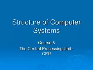
Memory Memory μP Address Data Commands I/O interface I/O interface I/O dev. I/O dev. Signals of a microprocessor – the System Bus
μP SVGA Mem Mem AGP Chipset N Net PCI Chipset S Keyboard Mouse Structure of a PC (a more realistic view)
Address signals Interrupt signals Micro-processor Bus arbitration signals Data signals Clock signal(s) Other signals (e.g. status, control) Command signals Power supply signals Typical signals for a microprocessor
Typical signals for a microprocessor • Address signals: A0-An • Used for specifying memory locations or I/O ports (registers) • Generated by the microprocessor to other components in order to address them (read or write operations) • The number of address lines determine the maximum addressing space of a microprocessor • Ex: 20 lines=> 1MB • 32 lines =>4GB • Data signals: D0-Dm • Bidirectional lines used to transfer instruction codes and data between the microprocessor and the other components of the system • The number of data lines is usually in accordance with the internal organization of the processor (there are also exceptions, see 8088, Pentium Pro) • The number of data lines determine the maximum width of a data transferred on a bus • Ex: 8, 16, 32, 64 lines
Typical signals for a microprocessor • Command and control signals • Command signals: • MRDC\, MWTC\, IORC\, IOW\, INTA\ • determine memory and interface read and write cycles • very important signals, • similar signals for any microprocessor • Control signals: ALE (Address Latch Enable), DEN (Data enable) • help controlling the address and data amplifiers • specific for every microprocessor • Interrupt signals: INTR, NMI • Clock signals: CLK, PCLK • Power supply signals: GND +5V, 3,3V
Instructions execution • Steps: • Instruction fetch • Operands read • Operation execution • Write the result • Seen from outside: • Instruction fetch cycle – read from the memory - mandatory • Operand(s) read - optional • Write the result - optional • Transfer cycle (on the bus) • a transfer on the bus that involve: • Processor and memory or • Processor and an I/O interface • A cycle has a fixed number of clock periods (determined by the microprocessors architecture) • it may be extended on request with an integer number of clock periods, if a slow module is addressed (e.g. EPROM memory) • A cycle is a sequence of signal activations on the bus (address, data and command) • a cycle is described by a time diagram
Read Memory Cycle A0-An valid address MRDC MWTC valid data D0-Dm taccess tcycle Write Memory Cycle valid address A0-An MRDC MWTC valid data D0-Dm taccess tcycle Time diagrams for transfers on a classical bus
Processors of the Intel x86 family • I8086 and I8088
I8086, I8088 • I8086 • 16 bits processor with 16 data lines, 20 address lines (1MB addressing space) • 40 pins integrated circuit • Supporting circuits: • 8087 – mathematic co-processor (floating point) • 8288 – bus controller • 88289 – bus arbiter • Structure: • EU –Execution Unit – dedicated for instruction execution • CU, ALU, general registers, state register • BIU – Basic Interface Unit – a unit responsible for the operations (transfer cycles) with the external bus • transfers instructions (in advance) and data • contains: • Special registers (segment registers, IP) • Instruction queue, bus amplifiers • 8088 • identical with 8086 but with 8 data signals on the external bus
I80286 • 16 bits processor • 16 data lines, 24 address lines (16MB addressing space) • Working modes: real and protected (privileged)
I80386 • 32 bits processor, 32 data lines, 32 address lines (4GB addressing space) • General registers extended to 32 bits • 2 extra segment registers (FS and GS) • Protected mode improved
I80486 • Integrates: processor + co-processor + MMU • Enables the use of cache memory • Protected mode improved
Pentium • Two pipelines: U (integers) and V (floats) • 64 bits external bus (for a 32 bits processor) • Versions: • Pentium –2 pipeline architecture • Pentium Pro • Pentium II - superscalara P6 architecture • Pentium III • Pentium IV – NetBurst architecture • I7, I5, I3 - multicore and hyperthreading
Pentium Processors • Pentium Pro • Superscalar P6 architecture (CPI<1) • Dynamic instruction execution: • Data flow analysis • Branch prediction • Speculative execution of instructions • Pentium II • MMX technology: • a SIMD execution unit dedicated for multimedia data • Parallel (SIMD) execution of arithmetic operations • 57 new MMX instructions • Pentium III • SSE2 technology • Parallel execution (SIMD) on floating point variables • good for 2D/3D graphics
P6 superscalar architecture • 3 autonomous units, 12 pipeline stages • Speculative execution
Instruction fetch and decoding unit • Fetch and decode instructions in advance • In-order unit • 3 instructions decoded /clock • Branch prediction • Components: • Decoder (3 units) • Address generator unit (next_IP) • Branch target buffer • Micro-operation sequencer • Alias registers allocator
Instruction dispatch and execute unit • Responsible for instruction execution • Out-of-order unit • 7 execution units + reservation station • IEU – Integer Execution Unit • FEU – Floating-point Execution Unit • MMX – Multimedia execution unit • AGU – Address generation unit • JGU – Jump generation unit
Retirement Unit • Reestablish the normal order of the instructions (of results) • In-order unit • Components: • MIU – memory interface unit • RRF – Retirement register file
Solving hazard cases in the P6 architecture • Control hazard: • complex branch prediction, BTB, next address predictor • out-of-order instruction execution • execute both branches of an if • Data hazard: • alias registers: renaming of registers and more internal registers (40) than those seen by the programmer • out-of-order instruction execution • data dependency tree • Structural hazard • multiple execution units (7 ALUs) • separate instruction and data cache • reservation stations • In essence it is an implementation of Tomasulo’s method
The P6 Bus • The main elements of the P6 bus: • the bus works in a synchronous mode; every signal is considered on clock signal edges • transfers are made through transactions that may be executed in parallel • it is a multi-processor bus; more processors on the same bus • block transfers are preferred • there are error detection and correction mechanisms • there are mechanisms that assure cache memory consistency • a new digital technology (different amplifiers) that assure high frequency transmissions on bus
Transfer on the P6 bus • Parallel transactions (pipeline) • Phases: • Arbitration– decides which master has access on the bus • Transfer request– specifies the request (read or write, start address, number of bytes) • Snooping– detect and solve cache inconsistencies • Error – detect and solve transmission errors (ECC – error correction code on data and parity on address and command signals) • Response – specifies the type of the answer (now, delayed, refused) • Transfer– data transfer in accordance with the request • Technology: GTL (instead of TTL)
Pentium IV –NetBurst Architecture (7th generation) • a 20 stage pipeline architecture • double compared with P6 • bus frequency is increased 4 times • 400MHz, with "quad pump“ technology, • 3.2Gbytes/s transfer speed • doubles the speed of the ALU, • 2 arithmetical operations are executed in every clock period; • the ALU works with a double frequency clock • the use of very high speed cache memory • Advanced Transfer Cache, that assures at 2GHz 64Gbytes/s data transfer • extension of the MMX technology • the SSE – Streaming SIMD Extension • 144 new SIMD instructions that extend the data width to 128 bits (16 bytes processed in parallel) • improvement of branch prediction with aprox. 30% • through the extension of the BTB unit and • increasing the instruction queue to 126 instructions
Pentium IV L2 Cache and control Interface with the external bus BTB Decoder Instruction fetch and decode Trace cache ROM Alias reg alocator Instr. queues for microoperations Schedulers Instruction scheduling and execution Reg. for „floats”Registers for „integers” ALU ALU-F ALU-F ALU ALU ALU AGU AGU L1 D-Cache The NetBurst Pentium IV architecture
Pentium IV • New tendencies: • Hyper-threading technology • two threads executed in parallel on the same core • Multi-core technology • more processors on the same chip • 64 bits architecture
Nehalem architecturemultiprocessor configuration Communication on QPI – QuickPath Interconnect Communication on FSB – Front side bus
Sandy bridge architecture • The north bridge (memory controller, graphics controller and PCI Express controller) is integrated in the same chip as the rest of the CPU. First models will use a 32-nm manufacturing process • Ring architecture - 256-bit/cycle • Two load/store operations per CPU cycle for each memory channel • New decoded microinstructions cache (L0 cache, capable of storing 1,536 microinstructions, which translates in more or less to 6 kB) • 32 kB L1 instruction and 32 kB L1 data cache per CPU core (no change from Nehalem) • L2 memory cache was renamed to “mid-level cache” (MLC) with 256 kB per CPU core • L3 memory cache is now called LLC (Last Level Cache), it is not unified anymore, and is shared by the CPU cores and the graphics engine • Next generation Turbo Boost technology • New AVX (Advanced Vector Extensions) instruction set • Up to 8 physical cores or 16 logical cores through Hyper-threading
Sandy bridge architecture 1 processor 4 cores 2 processor 8 cores/processor