Download
1 / 23
230 likes | 336 Views
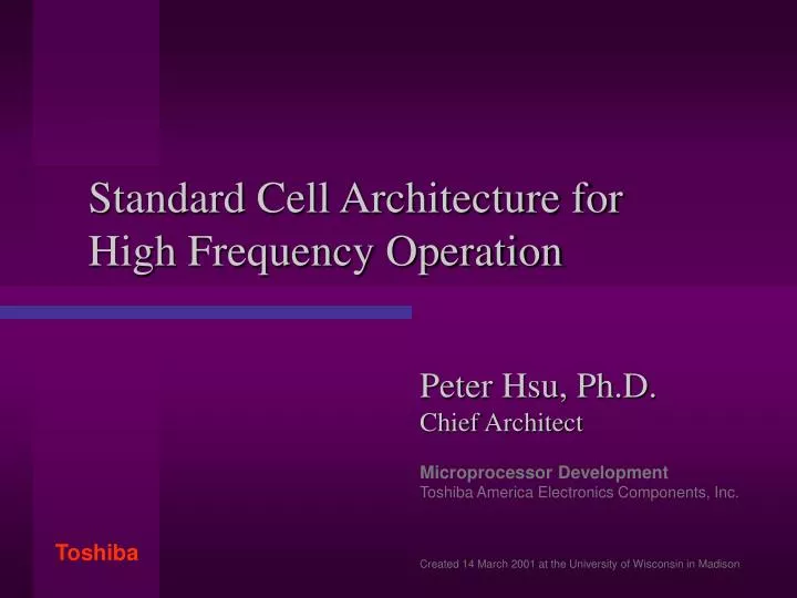
Standard Cell Architecture for High Frequency Operation. Peter Hsu, Ph.D. Chief Architect Microprocessor Development Toshiba America Electronics Components, Inc. Created 14 March 2001 at the University of Wisconsin in Madison. Disclaimer.

E N D
Standard Cell Architecture for High Frequency Operation Peter Hsu, Ph.D. Chief Architect Microprocessor Development Toshiba America Electronics Components, Inc. Created 14 March 2001 at the University of Wisconsin in Madison
Disclaimer • The ideas, data and conclusions presented here are solely those of the Author, and do not in any way represent Toshiba Corporation policy or strategy. Layout Architecture for High Frequency Operation
Introduction • High Frequency is Difficult! • Many Issues: • Signal Integrity, Power Dissipation, ... • My Approach: • Disciplined Methodology • Global Optimization • Outline • Layout • Circuits • Analysis Layout Architecture for High Frequency Operation
Layout Strategy • Leverage Advanced Technologies • Local Interconnect • Flip-Chip Area Array I/O • CAD Tool Compatibility • Parasitic Estimation, Extraction • Complex, High Frequency Designs • Robust Power Grid • Flexible Macro Embedding Layout Architecture for High Frequency Operation
300nm 300nm 150nm 150nm Metal Usage Dimensions are for nominal 0.12µm generation process Top Metal: Flip-Chip Solder Pads VDD 600nm 450nm Global Wires 900nm Signal Clock (2x) 450nm Via 300nm VSS Short 200nm Contact Local Interconnect (M0): Tungsten, Aluminum or Copper Layout Architecture for High Frequency Operation
Minimum Power Rail 6 Tracks From Edge VDD Cell Row Power Vias VDD VSS A A Local Interconnect U1 U2 VDD Z Z Minimum Pin Width 2 Tracks Pins Must Stagger VSS Smallest Cell 13 Tracks Double Height Cell Standard Cell Layout Unrelated Wire U1.A U1.Z Cell Row Power Vias (1 every 6 Tracks) Crosspoint Power Vias U2.Z U2.A Minimum Cell 3 Tracks Layout Architecture for High Frequency Operation
670µm 256 Rows 256 Columns Cell Array Decoder 256 Rows 256 Columns Cell Array 538µm 640µm Sense Amp. Sense Amp. 102µm 307µm 56µm Area Array I/O 1.2m I/O VDD Core VSS I/O VSS Core VDD Signal Largest SRAM Macro without sacrificing I/O (16 KBytes) Cell 2.5m2 225m pitch 225m 5 I/O Macro (50Km2 ) Layout Architecture for High Frequency Operation
I/O Macro Cell • Self-Contained • 5 Signals • VDDQ, VSSQ • ESD Protection • Latch-Up Ring • SoC Flexibility • Many I/O Types • Different Voltages • Routing Porosity • 50% Channels Free in Global Wiring Layers • Short Output Trace on Top Metal (Electromigration) Top Metal M6 M5 Free Routing Channels M4 M3 I/O Macro Use M0+M1+M2 Layout Architecture for High Frequency Operation
VSS VSS Bit Lines Signals VDD VSS Word Line #1 VDD Word Line #2 SRAM Metal Usage M2 M1 6-Transistor Cell (1.2 2.1 m) SRAM Macro Uses M0+M1+M2 M3 Global Wires (1 or 2 Pitch) CAD Tool Inserts M3:M2 Power Vias Layout Architecture for High Frequency Operation
Decoder Blocked Tracks Cell Array M3 Global Wires Sense Amp. Bit Lines Zigzag Minimizes Coupling from M3 Signals to M2 Word Lines when SRAM is Rotated Word Line Shielding Signals Signals Signals VDD VSS Layout Architecture for High Frequency Operation
Rationale • “Effective Area” • Actual Footprint + Routing Disturbance • Larger, More Porous Layout Faster • Bigger Transistors • More Space around Bit Lines • Shielding • SoC • Complex Microarchitecture • Many Small SRAMs Layout Architecture for High Frequency Operation
Circuit Design • Building Blocks • Latch Array • Malleable, Porous, Multi-Port SRAM • Dynamic Wire-OR Gate • High Fan-in, Safe, CAD Compatible • Power Dissipation • Double Edge Flipflop • 50% Clock Tree 30% Peak Chip-Wide • Interpolation Cells Layout Architecture for High Frequency Operation
D D CK CK Q Q E E E E D D D D Q Q Q Q G G G G Decoder D D D Q Q Q CK CK CK Decoder Write Pulse Generator Latch Array Write Data Latch + Tristate Driver Read Address Write Address May Buffer during Place&Route Combinatorial Read Path Write Enable Test Mode Read Data Layout Architecture for High Frequency Operation
D Q G D D _ G _ G _ Q _ Q Dynamic Wire-OR Gate Sized for Max. Length • Highest Leverage • Dynamic vs. Static • Safe, CAD Compatible • Limit Wire Length using Timing Driven Placement • No Dynamic Inputs Receiver Cell Keeper Output Clock Max. Length by Max-Load, Max-Transition Spec. Sized for 1 Input D1 Input DN Limit Max. N by Max-Fanout Spec. Clock Clock Sized for Max-Fanout Driver Cell Layout Architecture for High Frequency Operation
Double-Edge Flipflop • Low Power • Clock ½ Frequency • Light Clock Load • 2 Large + 4 Small • Small, Fast§ • 15P + 15N Transistors • Safe, Flexible • Fully Static • Supports Scan D Q Ck Switching Nodes with Constant “1” Data ______ §B. Nikolic, et.al., “Sense Amplifier-Based Flip-Flop,” ISSCC 1999. Layout Architecture for High Frequency Operation
Interpolation Cells Full Power 2/3 Power 5/6 Power For Post Route In-Place Optimization Same Footprint, Shorter Transistors 1X Cell 2X Cell 4X Cell Layout Architecture for High Frequency Operation
Analysis • Signal Integrity • Parasitics “Accurate By Construction” • Uniform Metal Density • Majority Coupling to Power Rails (Shielding) • Speed Yield • Balanced with Resources • Area, Power, Design Time • Goal: Adequate Confidence Layout Architecture for High Frequency Operation
VDD A A U1 U2 Z Z VSS Uniform Metal Density Post Route Metal Usage Algorithmically Generated Filled Metal Uniform Density on all Layers (except Local Interconnect) Layout Architecture for High Frequency Operation
Advantages • Design • Accurate Estimation • Capacitance has Low Variance • Known Coupling • 50% to Adjacent Power Line • Quick Feedback • Interconnect-Only Extraction is Accurate • Manufacturing • Uniform Etch Resist Loading Layout Architecture for High Frequency Operation
Same Asymmetric Rise-Fall Delays Delay Duty Cycle Slow Slow Same Size P Transistors Same Size N Transistors Elongates Shrink Layout Architecture for High Frequency Operation
Pros and Cons • Advantages • More Compact Cells, Faster Circuits • Disadvantages • Need Careful Analysis, Greater Margin • Strategy: • Main Library • Asymmetric, “No Wasted Space” • Symmetric Subset • Gated Clocks, Write Pulse Buffering, ... Layout Architecture for High Frequency Operation
Speed Yield Management Fast P Hold Time Failures Target Design and Characterize Library Here “Four Corner” Analysis Correct Operation Process Center Slow N Fast N Mature Process Variation Possibly Impossible to Meet Performance Goal, or Needlessly High Effort Setup Time Failures Maximum Process Variation Slow P Transistors Layout Architecture for High Frequency Operation
Conclusions • “Precision Physical Design” • Global • Power Grid • Macro Routing Porosity • Methodical • Signal Integrity • Parasitic Extraction • Timing Uncertainties (Coupling) • Confident • Correctness and Speed Layout Architecture for High Frequency Operation