Download
1 / 17
220 likes | 563 Views
Signal Conditioning. Yuchen Chai, Pradeep Shenoy , Philip T. Krein. What Is Signal Conditioning.

E N D
Signal Conditioning Yuchen Chai,PradeepShenoy, Philip T. Krein
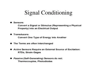
What Is Signal Conditioning • Many applications require environment or structural measurements, such as temperature and vibration, from sensors. These sensors, in turn, require signal conditioning before a data acquisition device can effectively and accurately measure the signal. Key signal conditioning technologies provide distinct enhancements to both the performance and accuracy of data acquisition systems.
Our Signal ConditioningPreliminary Design with Bread Board • Our Circuit Specifications 1.16 parallel signal inputs 2.Input Voltage magnitude is around 20V with some ripples 3. Output signal should meet Analog to Digital converter requirements which has 0 – 3.3V input range 4.Need low-pass filter
Our Signal ConditioningPreliminary Design with Bread Board • Our amplifier choice: AD8226: Wide Supply Range, Rail-to-Rail Output Instrumentation Amplifier Flexible gain range from 1 to 1000 (really what we want in our circuit) • Our filter choice: First-Order low pass filter with LM124/LM224/LM324/ LM2902:Low Power Quad Operational Amplifiers
Our Signal ConditioningPreliminary Design with Bread Board • Bread board layout at the beginning with several bugs
Our Signal Conditioning Design • 1st step – Amplification • Amplifiers increase voltage level to better match the analog-to-digital converter (ADC) range, thus increasing the measurement resolution and sensitivity.
Our Signal Conditioning Design • Test instrumentation amplifier functionality We did not find AD8226 in ECE workshop, but we choose AD622 Low Cost Instrumentation Amplifier (seems ok) and decided to test it functionality first
Our Signal Conditioning Design • Desired output (Red) from instrumentation amplifier and input (Green) with AD622 +10V power supply
Our Signal Conditioning Design • Our real output (Red) from instrumentation amplifier and input (Green) with AD622 +10V power supply :
Our Signal Conditioning Design • Output is distorted, but why? After changing the DC offset, we found that this is because we set the cutoff voltage(also means the supply voltage to AD622) from 0 V – 10V (with only Pin7 connected). When the mean value of the input voltage is 1V-2V below 10V or 1V-2V above 0V, the output is the clip version of the input. • How to solve it? Really Easy! Use Pin4 to give AD622 -10V to +10V power supply which can give our circuit more range. Some graphs are attached here.
Our Signal Conditioning Design • 2nd step - Filtering • Test the functionality We chose LM124 low power quad operational amplifier to act as a buffer and test its functionality, and we found it works correctly in the range of our input.
Our Signal Conditioning Design • “First-Order low pass filter” connect to the output from the instrumentation amplifier • we found the output signal from instrumentation amplifier is distorted which was not what we wanted to see • How to solve it? Really easy! • Instead of that complicated design, we choose to use “Passive low pass filter” which is much easier
Our Signal Conditioning Design • To make it more flexible with users’ requirements, we used a Trim potentiometer(small Bluebox) to give a wide range of output from the low pass filter, and we got the desired result.
Our Signal Conditioning Design All Done! • Output from filter (RED) at 725.7mV • Output from instrumentation amplifier (BLACK) • Input (GREEN) • Smoother output voltage (RED) at 1.463V by changing trim potentiometer:
Summary • We found the AD662 and LM124 fit our specification and can be used in PCB design for the signal conditioning circuit. I am still searching the parallel trim potentiometer to change the input voltage range simultaneously. Next step is to design the PCB layout through software, order components from manufacturers, and build the PCB.
Continuous Study • 1. PCB design on Eagle • 2. Order the PCB board!
Selected Reference “Operational Amplifiers and Signal Conditioning”, http://cnx.org/content/m13778/latest/ “What is Signal Conditioning? ”, National Instruments, http://zone.ni.com/devzone/cda/tut/p/id/10630 “LM124 Low Power Quad Operational Amplifier”, National Instruments, http://www.national.com/mpf/LM/LM124.html#Overview “AD622 Low Cost Instrumentation Amplifier”, Analog devices, http://www.analog.com/en/specialty-amplifiers/instrumentation-amplifiers/ad622/products/product.html “AD8226: Wide Supply Range, Rail-to-Rail Output Instrumentation Amplifier”, Analog devices, http://www.analog.com/en/specialty-amplifiers/instrumentation-amplifiers/ad8226/products/product.html