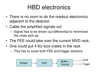
HBD Electronics
Comprehensive review of the HBD CDR's preamp and cable driver, schematics, testing results, and electronics chain. It includes specifications, block diagrams, component details, and insights on FEM blocks and signal flow.

HBD Electronics
E N D
Presentation Transcript
HBD Electronics • Preamp/cable driver on the detector. • Specification • Schematics • Test result • Rest of the electronics chain located in the rack. • Cable • Block diagram • Individual components • HBD LL1 trigger • Outlook HBD CDR Review
Charge Preamp with On-Board Cable Driver(IO1195-1-REVA) • Features: • +/- 5V power supply. • 165 mW power dissipation. • Bipolar operation (Q_input = +/- ) • Differential outputs for driving 100 ohm twisted pair cable. • Large output voltage swing -- +/- 1.5V (cable terminated at both ends) • (+/- 3V at driver output) • Low noise: Q_noise = 345e (C_external = 5pF, shaping = .25us) • (Cf = 1pF, Rf = 1meg) • Size = 1.04” x 0.775” 10pins • Preamp output (internal) will operate +/- 2.5V to handle large pile-up. HBD CDR Review
IO1195-1-REVA HBD CDR Review
Test with GEM Detector PA Pulse Trace on Scope Pulser Input(1.2pF)~ 13mV100,000 e-’s • Input capacitance ~ 0.0 pF?? • 20 pe x 5E3 (gain) ~ • 100,000 electron input into • pre-amp • Baseline Noise~ 1100e-’s • after background is subtracted • off. s(Baseline Noise) ~1100 e-’s PA Output~48mV PA Pulse Height Spectrum B.Azmoun HBD CDR Review
Use 2MM Hard Metric cable to move signals between preamp/FEM 2mm HM connector has 5 pins per row and 2mm spacing between pins and rows There are two types of cable configuration: *100 ohms parallel shielded cable 50 ohms coaxial cable Signal arrangement S- S+ G S+ S- Our choice is This gives us signal density 2mm x 10mm for every 2 signals. Same type of cables will be used for L1 trigger data. HBD CDR Review
HBD FEM • 48 channels per FEM • 12(11) bits 60MHz sampling per channel. • 3 bits LL1 data output per channel • 7 individual threshold levels per channel • Optical output to DCM, 6xbeam crossing rate(~60MHz). • Use commercial 8b/10b chip (TI) plus optical transceiver • 6UX220mm card size • Interface module • GTM (clock, L1 trigger etc.), Ethernet interface for slow download. • Control test pulse. • 6U x 220 mm card size • HBD readout will fit into 3 6U crates • HBD LL1 module potentially could fit into one 6U crate. HBD CDR Review
FEM Block Diagram FPGA Receive/buffer ADC data Format triggered Events Generate L1 Primitives Receive timing /clocks 8 Channels 65 MHz 12 bits ADC Differential Receiver Connector Data path LL1 trigger FEM Crate Diagram Trigger data interface FEM FEM FEM FEM Optical Detector signals GTM/Ethernet DCM HBD CDR Review
The differential receiver Use Analog Device AD8138 receiver set up as unity gain Simulation result For 16fc input charge Total voltage On the cable Total voltage Seen by ADC ADC has 1V range Max ADC range is about ~10 time of 16fc ADC +/- inputs HBD CDR Review
The 8 channel 12 bits 65MHzADC The ADC receives differential signals The Vcommon is 1.5V The +/- input can swing from 1V to 2V + side 2V, - side 1V -> highest count - side 2V, + side 1V -> lowest count Our +/- input will swing from 1.5 to 2V/ 1 to 1.5V we will only get 11 bits out of 12 bits 16fc will be roughly sitting 200 count We will run the ADC at 6X beam crossing clock 6X9.4 MHz = 56.4 MHz or ~17.7ns per samples HBD CDR Review
FPGA • Receive ADC data, provide L1 delay, Multiple L1 triggered events, format data, generating L1 trigger primitives, transfer L1 trigger data ,manage clocks and test pattern etc. • 48 channel of serial ADC => 48 *720 Mbits/sec or 34 Gbits/sec need to be received. • We choice Altera Stratix II 90nm EP2S60 1020 pins to received the ADC data. HBD CDR Review
Signal Flow current progress on the FEM board Differential receiver Majority of boards is set We now try to deal with the power issues +3.3 for ADC +/- 2.5V for receiver FPGA needs +3.3V, +2.5V, +1.2V Signal input EP2S60 FPGA ADC HBD CDR Review
HBD data to DCM • 12 samples per channel • Cover 2 beam crossing • Assume the optical will run 6X beam crossing rate. • 48 channel will take ~16.6 ns*48*12=9.6 microsec. • We will merge 4 FEMs’ data into one optical link in un-multiplexed mode HBD CDR Review
HBD L1 trigger • Each FEM output 3 bits per channel, 7 threshold setting. • Total bandwidth is 3*48 channel*9.6MHz ~1.4 GHz (~1.7 GHz optical bandwidth) • Multiplex FEM L1 data into 3 differential pairs + 1 clock pair cable • Use 4mm vertical space. • The HBD LL1 crate could locate within the HBD FEM rack. • Each arm of the HBD has 12 panels. Each panel has 96 channels. Each FEM cover 48 channels. • Each LL1 covers 24 FEM’s data • Generic LL1 has 16 optical inputs • The Stratix II EP2S60 chip can receive 8 FEM inputs. 3 chips could cover 24 FEM’s data. • We should have enough logic to deal with reasonable trigger algorisms. • HBD LL1 decisions will be send to GL1 and LL1 calculation result will be send to DCM. HBD CDR Review
Outlook • The prototype FEM layout will be done soon. • We need to work on the interface board and dataway. • Test can be underway once these boards exist. • Need to deal with how to receive optical data in the DCM end. • Probably with a special daughter card HBD CDR Review