Download
1 / 26
320 likes | 634 Views
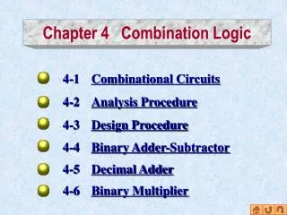
Chapter 5 Combination Logic. 5-1 Basic Combinational Logic Circuits. 5-2 Implementing Combinational Logic. 5-3 Design Procedure. 5-4 Characters of Nand and Nor. 5-5 Nand and Nor Implementation. 5-6 Troubleshooting. 5-7 Programmable Logic Devices. 5-8 Digital System Application.

E N D
Chapter 5 Combination Logic • 5-1 Basic Combinational Logic Circuits • 5-2 Implementing Combinational Logic • 5-3 Design Procedure • 5-4 Characters of Nand and Nor • 5-5 Nand and Nor Implementation • 5-6 Troubleshooting • 5-7 Programmable Logic Devices • 5-8 Digital System Application
Digital Logic Logic circuits Combinational circuits Sequential circuits
x1 x2 xn Combinational circuits Z1 Z2 Zn 5-1 Basic Combinational Logic Circuits Z1=f1(x1,x2, …xn) Z2=f2(x1,x2, …xn) Zn=fn(x1,x2, …xn)
5-2 Implementing Combinational Logic The first step in the analysis is to make sure that the given circuit is combinational and not sequential. The diagram of a combinational circuit has logic gates with no feedback path or memory elements.
≥ ≥ ≥ 1 1 1 A F B 1 1 A B A+B A +B
5-2 Implementing Combinational Logic • Truth Table The truth table can be derived from the Boolean function and logic diagram. Once we have the truth table for the circuit, we can also directly write a logic expression-the canonical sum or product-if we wish.
5-3 Design Procedure The Design procedure involves the following steps: 1.From the specification of the circuit,determine the required number of inputs and outputs and assign a symbol to each. 2. Derive the truth table that defines the required relationship between inputs and outputs. 3. Obtain the simplified Boolean functions for each output as a function of the input variables. 4. Draw the logic diagram and verify the correctness of the design.
5-3 Design Procedure Example: Use NAND gates to realize the follow function
Example: Use NAND gates to realize the follow function Conclusion: AB CD 00 01 11 10 00 01 11 10
A A & & 1 B & & A 1 & & F F B B & & 1 C C & & D D 1
A & & D & F & C & B
We can get another NAND-NAND express Only use 4 NAND gates Since
5-4 Characters of Nand and Nor Two-Level Implementation The procedure for implementing a Boolean function with two levels of NAND gates is as follows: • Simplify the function and express it in sum of products. • Draw a NAND gate for each product term of the expression that has at least two literals.
5-4 Characters of Nand and Nor The procedure for implementing a Boolean function with two levels of NAND gates is as follows: • Draw a single gate using the AND-invert or the invert-OR graphic symbol in the second level, with the inputs coming from outputs of first level gates. • A term with a single literal requires an inverter in the first level. It can also be connected directly to an input of the second level NAND gate.
5-5 Characters of Nand and Nor NAND Circuits The Realtionship between AND,OR and NAND gates.
F= x +y + z =(xyz) F= (xyz) 5-5 Nand and Nor Implementation Two equivalent graphic symbols for the NAND gate are shown below, Logically equivalent
5-5 Nand and Nor Implementation Example: implement the following Boolean function with NAND gates:
AB CD 00 01 11 10 00 01 11 10
5-5 Nand and Nor Implementation Multilevel NAND Circuits The procedure for converting a multilevel AND-OR diagram into an all-NAND diagram using mixed notation as follows: • Convert all AND gates to NAND gates with AND-inverter graphic symbols. • Convert all OR gates to NAND gates with inverter-OR graphic symbols. • For every bubble that is not compensated by another small circle along the same line, insert an inverter or complement the input literal.
5-5 Nand and Nor Implementation Example:
5-5 Nand and Nor Implementation NOR Implementation The NOR operation is the dual of the NAND operation. Therefore, all procedures and rules for NOR logic are the dual of the corresponding procedures and rules developed for NAND logic.
F= (A+B) +(C+D) =[ ( A+B) (C+D) ] F= (AB) (CD)=(AB+CD) 5-5 Nand and Nor Implementation Wired logic
Y4 Y6 Y5 STC Y3 Y7 Y1 STB Y0 Y2 CP BIN/OCT 0 1 2 3 1 2 4 A0 Q1 A1 A2 4 5 6 7 Q2 & STA EN Q3 Q4 Z 5-6 Troubleshooting
VDD CP + + TG vI vO C R - - CP 5-7 Programmable Logic Devices