Download
1 / 177
1.79k likes | 1.97k Views
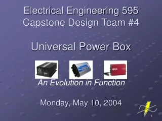
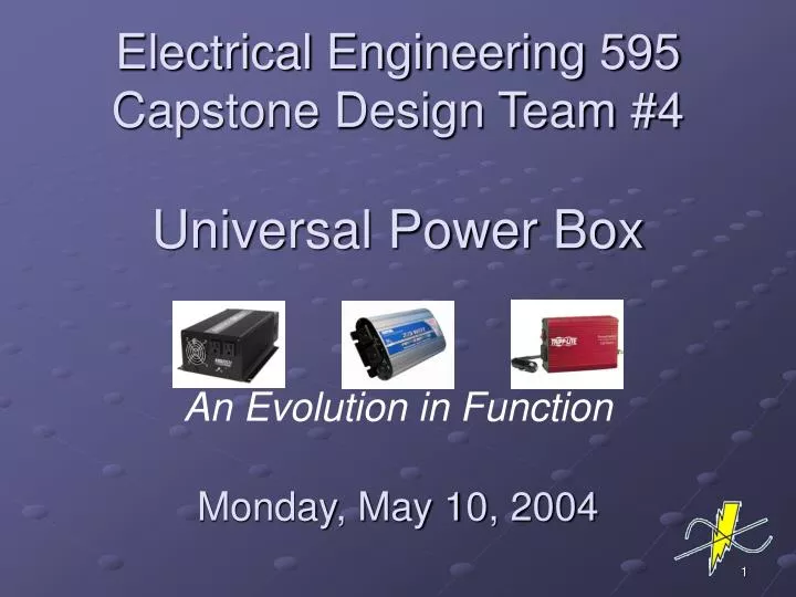
Electrical Engineering 595 Capstone Design Team #4 Universal Power Box. An Evolution in Function. Monday, May 10, 2004. Staff (1). Gerry Callison, BSEE Expertise: Power Systems, Digital Design, Presentation Experience: 3 years experience at Johnson Controls Maria Schlicht, BSEE

E N D
Electrical Engineering 595 Capstone Design Team #4 Universal Power Box An Evolution in Function Monday, May 10, 2004
Staff (1) • Gerry Callison, BSEE • Expertise: Power Systems, Digital Design, Presentation • Experience: 3 years experience at Johnson Controls • Maria Schlicht, BSEE • Expertise: Micro controllers, PLCs, Project Management, Technical Writing, Language Skills • Experience: 8 years experience at Rockwell Automation • Ethan Spafford, BSEE • Expertise: RF, Circuit Design, Optical Communication, PSpice Software
Staff (2) • Matt Risic, BSEE/BSCS • Expertise: High Level Programming, Assembly, Computer Networks, Computer Organization • Experience: Two summers interning at Philips Advance Transformer • Vanessa White, BSEE • Expertise: Digital Design, Micro controllers, PLC Logic • Experience: One year experience at Harley Davidson
Project Abstract • With the immense selection of electrical devices used in everyday lives, there can be much need to convert between one type of power source into another. The Universal Power Box (UPB) combines many types of conversions into one product. • Cost, reliability, accuracy and safety were key aspects in the scope of this project.
Product Description • The user attaches a power source to the UPB, then enters a desired output power type and level. • The UPB senses the type of power the user inputs. • The UPB utilizes a Flyback DC to DC converter and an H-bridge inverter which doubles as a full-wave rectifier for power conversion. • The power converters are run by a microprocessor, which takes input from a variety of feedback sensors. All converters are pulse-width modulated.
Product Feature Set • The UPB can convert AC to DC, DC to AC, and DC to DC. • The user interacts with the UPB through an LCD and numeric keypad. • The UPB draws its internal power supply from the input power. • The UPB has a Total Harmonic Distortion sufficiently low for consumer electronics applications. • The UPB has a weight, size, and durability that allows it to be portable. • Many different power adapters available, but none known that combine AC-DC, DC-AC, and DC-DC in one product
Target Market • This product is being developed for use with consumer electronics in the North American environment. • Product NOT approved for Medical Applications • This product will be distributed through electronics and hardware retailers. • Common applications include: • Creating 120 VAC from a car outlet (for both 14Vdc and 42Vdc systems). • Replacing consumer electronic AC to DC adapters.
Product Performance Requirements • Input voltage ranges: • 14-50Vdc • 108-132VAC @ 60Hz • Maximum input current: 7 amps • Output power: 75 watts • Output voltage ranges: • 14-50Vdc • 108-132VAC @ 60Hz • Maximum output current: 5 amps • Total Harmonic Distortion < 5%
Product Standard Requirements • 0-50 degrees Celsius • 0-70% RH • Maximum product size 2000 cm3 • Maximum product mass 2kg • Maximum parts count 200 • Greater than 95% reliability for 6 months
AC to DC operation overview • AC voltage applied to I/O AC. • Uncontrolled Inverter/Rectifier converts AC to DC. • DC-DC converter adjusts output DC voltage to user-defined level.
DC to DC operation overview • User inputs DC to I/O DC. • DC-DC converter adjusts DC to user defined level of DC. • Inverter/Rectifier switches configure to pass through output DC without altering it.
DC to AC operation overview • User inputs DC through I/O DC. • DC-DC converter adjusts level of DC necessary for proper AC output. • Inverter/Rectifier runs PWM switching to output AC.
Power Control Matt Risic
Block Purpose • The Power Control is the center of the Universal Power Box • The programming is responsible for converting input data from the DC Sensor and relaying the PWM waveform to the Inverter Rectifier • Microprocessor will control the LCD display based on user input from the keypad • Input will be taken from the IC driver connected to the keypad
Standard RequirementsControl • Humidity Range 0%RH to 70%RH • Block Cost <$15 • Parts Count <20 • Block Size <48cm2 • Block Mass <95.5 grams • Max Power Consumption <20W • Operating Temperature Range 0C to 75C • Storage Temperature Range 0C to 75C • Operating Humidity 0-70% • Reliability (MTBF) 3 Years
Performance RequirementsControl • Input Voltage +3.3V (+/- 3%) • Full Scale Output Voltage +3.3V (+/- 3%) • Minimum speed 1Mhz • Desired Memory 1K SRAM • Programming Language C and Assembly • Number of Registers 32
Input/Output Voltages Internal Sensors Gate Signals AC Sensor DC-DC Converter Vmeas AC 0 / 3.3V 0-3.3V Vmeas I1 Vmeas I2 DC Sensor Inverter Rectifier Gate Signals 0-3.3V 0-3.3V Vmeas DC 0 / 3.3V Power Control 0-3.3V Power Source 3.3V AC I/O Control Power 0 / 3.3V Vpower 2 Bits DC I/O Relay / Duty Cycle IC Osc Input Output 0 / 3.3V 2 Bits 4 Bits 4 Bits Vpower Keypad LCD Display
Microprocessor Selection • Atmel ATMega169v Microprocessor • 1 MHz Clock Speed • Advanced RISC Architecture • 130 Instruction Set • C and Assembly Coding • 32 x 8 General Purpose Registers • 16KB Programmable Flash • 512 Bytes EEPROM • 1KB SRAM • 64 Pin Chip
ATMega169v Operating Conditions • Operating voltage between 1.8-5.5V • Operating temperature between -40 to +85 degrees Celsius • Up to 1 MHz Clock Speed • Power Consumption • At 1MHz consumes 1.8V, 400uA • At 32 kHz consumes 1.8V, 20uA • Power-down Mode is 0.5uA at 1.8V
MPU Pin Configuration • Port A (PA7-PA0) Bi-directional I/O port with pull-up resistors COM0:3 and SEG0:3 for LCD Controller • Port B (PB7-PB0) Bi-directional I/O port with pull-up resistors • Port C (PC7-PC0) Bi-directional I/O port with pull-up resistors • Port D (PD7-PD0) Bi-directional I/O port with pull-up resistors • Port E (PE7-PE0) Bi-directional I/O port with pull-up resistors • Port F (PF7-PF0) Analog inputs to A/D Converter • Port G (PG7-PG0) 5 bit bi-directional I/O port with pull-up resistors • LCDCAP (Pin 1) External Capacitor Reservoir for LCD Display • RESET (Pin 20) Reset Pin • VCC (Pins 21,52) +3.3V Power Pin • AVCC (Pin 64) Supply Voltage for Port F and A/D Converter • GND (Pins 22,53,63) Ground Pin
+3.3V Ground 0/3.3V to AC I/O 0/3.3V to DC I/O 0/3.3V AC 0/3.3V DC 0/3.3V Sensor 0/3.3V sensor Ground +3.3V LCD Pin 4 LCD Pin 5 LCD Pin 6 470nF Cap Bit 0 Control Power Bit 1 Control Power LCD Pin 7 LCD Pin 8 LCD Pin 9 LCD Pin 10 LCD Pin 11 LCD Pin 12 LCD Pin 13 LCD Pin 14 0 / 3.3V Inverter Rectifier 0 / 3.3V Inverter Rectifier 0 / 3.3 V Inverter Rectifier 0 / 3.3V Inverter Rectifier 0 / 3.3V DC-DC Converter 0 / 3.3 V DC-DC Converter Reset +3.3V V Ground Driver Pin 16 Driver Pin 17 Keypad Pin 1 Keypad Pin 2 Keypad Pin 3 Keypad Pin 4
Programming Software • AVR Studio 4.08 • Integrated Coding, Compiling and Debugging Software • Configurable Memory • Support for C, Pascal, BASIC and Assembly • Simulate Port Activity Logging and Pin Input
Programming Software • AVR LCD Visualizer • Create and modify LCDs with editor • Debug and visualize with AVR plug-in • Real run-time updates
Output Program Flowchart WELCOME TO UPB! 1.DC-DC 2.AC-DC 3.DC-AC NO (1-3?) YES NO NO (3?) (2?) (1?) YES YES YES DC-DC ENTER DC OUTPUT AC-DC ENTER DC OUTPUT DC-AC 120V AC NO NO (14-50?) (14-50?) YES YES AC-DC XXV DC DC-DC XXV DC
Input Program Flowchart Regular Program Execution NO Key press? YES Interrupt Cycle Import Keystroke Decode Input in MPU Send to PWM Output to LCD End Interrupt Cycle
Block Component Cost • ATMega169v microprocessor - $10.81 • STK500 Board - $79.00 *Prototype Only • STK502 Expansion Board - $99.00 *Prototype Only • AVR Studio 4.08 – FREE • AVR Studio 4 Service Pack – FREE • AVR LCD Visualizer - FREE
Reliability Prediction 3 year reliability: 99.155%
User Interface Maria Schlicht
User Interface Overview • The user interface will contain a 12-key numeric keypad to enter the voltage desired by the user. It will also contain a 16 x 2 LCD display. • The inputs include: • The User can select three modes of operation: (AC–DC, DC-AC & DC-DC) • User can defined Level/Type of power • The User will have access to review or modify the terminal settings using NUMERIC keys to navigate through the configuration screens. • Electrical Safety for User
LCD Operating Values: LCD Supply Voltage Range: 2.6 -3.0V Input High Voltage VIH: 2.2-5.1V Input Low Voltage VIL: 0.65V Output High Voltage VOH: 2.3V Output Low Voltage VOL: 0.5V Max. Input Current IDD: 1.2mA Operating Temperature TOPR: 0°C - 50°C Storage Temperature TSTG: 0°C - 60°C Viewable 1 feet. User Interface Performance Requirements
User Interface Performance Requirements • EDE 1144 Keypad Encoder IC: • Supply Voltage: 3.0 V • Max. Current sunk by an output pin: 3.0 mA • Max. Current source by an output pin: 5.0 mA • Max. Current source by an output pin: 5.0 mA • Max. Current sunk by all 3 column inputs: 5.0 mA • Max. Current source by all 4 row outputs: 5.0 mA • Keypad Operating values: • Max. output current: 5.0 mA • Min. Operating Humanity Rage <95%, non-condensing
User Interface Block Diagram Input (Keypad) ATmega169 (Process) Output Display (LCD) DISPLAY MENU • DC-DC 2. AC-DC • DC-AC
User Interface Controls: 12-button keypad: Digits 0-9, pound sign, and Start key. Safety Features: Illuminated display indicates voltage present Temperature range as specified by overall product Components to be chosen to comply with temperature requirements Hand Assembly: Keypad and LCD display manually assembled, all other components can be automatically installed. Societal/Legal/Monetary Aspects: Pushbuttons (ergonomic & friendly) Material Degradation Rust and corrosion Suitable for electrical conditions Disposability/Recycle ability: Parts recyclable as PCB assembly Reliability: Prototype: Length of project Production: 1 yr @ 2% 5 yrs @ 10% User Interface Productization Requirements
64-QFP socket (ATmega169) • QFP bread boarding adapter with Aprilog CL production socket. • The socket permits insertion and removal of the package without soldering, thus making the devices, as well as the adapter re-useable. • The 64-QFP package can be plugged into a standard production 64-pin DIP socket or directly into solder less breadboard.
User Interface Failure Analysis • πT = Temperature Stress Factor • πV = Electrical Stress Factor • πE = Environmental Factor • πQ = Quality Factor
Inverter-Rectifier Gerry Callison