Download
1 / 5
111 likes | 469 Views
Electronic Packaging. Electronic packaging is everything needed to turn integrated circuits into electronic systems Power supplies Chip packaging Circuit boards Passive components (capacitors, resistors, inductors) Heat removal Human interfaces (keyboards, screens)

E N D
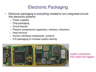
Electronic Packaging • Electronic packaging is everything needed to turn integrated circuits into electronic systems • Power supplies • Chip packaging • Circuit boards • Passive components (capacitors, resistors, inductors) • Heat removal • Human interfaces (keyboards, screens) • 3-D packaging to increase system density Inside a cell phone. EEs make this happen.
Chip Packages • Chip packages allow tiny pads on the IC to be connected to the circuit board. • There are many kinds of packages. • Reliability, cost, and performance are major engineering challenges.
Circuit Boards • Circuit boards connect all system components together, sometimes with thousands of mass-produced conductors fabricated on multiple layers. • Copper and epoxy reinforced with fiberglass are the most common materials. • Higher density ICs require boards with more wiring in less space. • Tiny vias connect the wiring on various layers.
Passive Components • Passive components, particularly capacitors, take up a lot of room in portable electronics. • Technologies being developed at UA aim to integrate these devices inside circuit boards, reducing area and volume.
UA is a national leader among colleges in turning IC chips into systems by 3-D stacking with dense through silicon via (TSV) interconnects. 3-D Systems Research Student researchers process wafers in the HiDEC cleanroom, a unique fabrication facility Cross section of copper filled vias to be used as interconnects. Each via is 1/3 the diameter of a hair!