Download
1 / 24
240 likes | 387 Views
Learn about drawbacks of single-cycle, benefits of multicycle and multiple-cycle implementations in computer architecture. Understand the stages involved like instruction fetch, decode, ALU execution, memory access, and more.

E N D
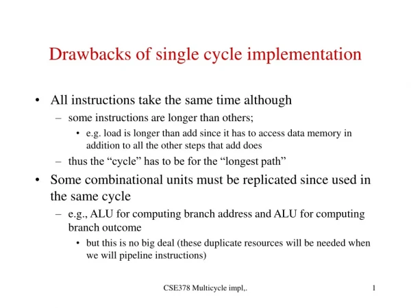
Drawbacks of single cycle implementation • All instructions take the same time although • some instructions are longer than others; • e.g. load is longer than add since it has to access data memory in addition to all the other steps that add does • thus the “cycle” has to be for the “longest path” • Some combinational units must be replicated since used in the same cycle • e.g., ALU for computing branch address and ALU for computing branch outcome • but this is no big deal (these duplicate resources will be needed when we will pipeline instructions) CSE378 Multicycle impl,.
Alternative to single cycle • Have a shorter cycle and instructions execute in multiple (shorter) cycles • The (shorter) cycle time determined by the longest delay in individual functional units (e.g., memory or ALU etc.) • Possibility to streamline some resources since they will be used at different cycles • Since there is need to keep information “between cycles”, we’ll need to add some stable storage (registers) not visible at the ISA level • Not all instructions will require the same number of cycles CSE378 Multicycle impl,.
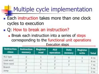
Multiple cycle implementation • Follows the decomposition of the steps for the execution of instructions • Cycle 1. Instruction fetch and increment PC • Cycle 2. Instruction decode and read source registers and branch address computation • Cycle 3. ALU execution or memory address calculation or set PC if branch successful • Cycle 4. Memory access (load/store) or write register (arith/log) • Cycle 5 Write register (load) • Note that branch takes 3 cycles, load takes 5 cycles, all others take 4 cycles CSE378 Multicycle impl,.
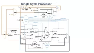
Instruction fetch • Because fields in the instruction are needed at different cycles, the instruction has to be kept in stable storage, namely need to introduce an Instruction Register (IR) • The register transfer level actions during this step IR Memory[PC] PC PC + 4 • Resources required • Memory (but no need to distinguish between instruction and data memories; later on we will because the need will reappear when we pipeline instructions) • Adder to increment PC • IR CSE378 Multicycle impl,.
Instruction decode and read source registers • Instruction decode: send opcode to control unit and…(see later) • Perform “optimistic” computations that are not harmful • Read rs and rt and store them in non-ISA visible registers A and B that will be used as input to ALU A REG[IR[25:21]] (read rs) B REG[IR[20:16]] (read rt) • Compute the branch address just in case we had a branch! ALUout PC +(sign-ext(IR[15:0]) *4 (ALUout is also a non-ISA visible register) • New resources • A, B, ALUout CSE378 Multicycle impl,.
ALU execution • If instruction is R-type ALUout A op. B • If instruction is Immediate ALUout A op. sign-extend(IR[15:0]) • If instruction is Load/Store ALUout A + sign-extend(IR[15:0]) • If instruction is branch If (A=B) then PC ALUout (note this is the ALUout computed in the previous cycle) • No new resources CSE378 Multicycle impl,.
Memory access or ALU completion • If Load MDR Memory[ALUout] (MDRis theMemory Data Register non-ISA visible register) • If Store Memory[ALUout] B • If arith Reg[IR[15:11]] ALUout • New resources • MDR CSE378 Multicycle impl,.
Load completion • Write result register Reg[IR[20:16]] MDR CSE378 Multicycle impl,.
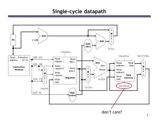
Streamlining of resources (cf. Figure 5.26) • Comparing data path with that of a single cycle implementation • No distinction between instruction and data memory • Only one ALU • But a few more muxes and registers (IR, MDR etc.) CSE378 Multicycle impl,.
Control Unit for Multiple Cycle Implementation • Control is more complex than in single cycle since: • Need to define control signals for each step • Need to know which step we are on • Two methods for designing the control unit • Finite state machine and hardwired control (extension of the single cycle implementation) • Microprogramming (read the CD about it) CSE378 Multicycle impl,.
What are the control signals needed? (cf. Fig 5.27) • Let’s look at control signals needed at each of 5 steps • Signals needed for • reading/writing memory • reading/writing registers • control the various muxes • control the ALU (recall how it was done for single cycle implementation) CSE378 Multicycle impl,.
Instruction fetch • Need to read memory • Choose input address (mux with signal IorD = 0) • Set MemRead signal • Set IRwrite signal (note that there is no write signal for MDR; Why?) • Set sources for ALU • Source 1: mux set to “come from PC” (signal ALUSrcA = 0) • Source 2: mux set to “constant 4” (signal ALUSrcB = 01) • Set ALU controlto “+” (e.g., ALUop = 00; How about function bits?) CSE378 Multicycle impl,.
Instruction fetch (PC increment; cf. Figure 5.28) • Set the mux to store in PC as coming from ALU (signal PCsource = 01) • Set PCwrite • Note: this could be wrong if we had a branch but it will be overwritten in that case; see step 3 of branch instructions CSE378 Multicycle impl,.
Instruction decode and read source registers • Read registers in A and B • No need for control signals. This will happen at every cycle. No problem since neither IR (giving names of the registers) nor the registers themselves are modified. When we need A and B as sources for the ALU, e.g., in step 3, the muxes will be set accordingly • Branch target computations. Select inputs for ALU • Source 1: mux set to “come from PC” (signal ALUSrcA = 0) • Source 2: mux set to “come from IR, sign-extended, shifted left 2” (signal ALUSrcB = 11) • Set ALU controlto “+” (ALUop = 00) CSE378 Multicycle impl,.
Concept of “state” • During steps 1 and 2, all instructions do the same thing • At step 3, opcode is directing • What control lines to assert (it will be different for a load, an add, a branch etc.) • What will be done at subsequent steps (e.g., access memory, writing a register, fetching the next instruction) • At each cycle, the control unit is put in a specific state that depends only on the previous state and the opcode • (current state, opcode) (next state) Finite state machine(cf. CSE370, CSE 322) CSE378 Multicycle impl,.
The first two states • Since the data flow and the control signals are the same for all instructions in step 1 (instr. fetch) there is only one state associated with step 1, say state 0 • And since all operations in the next step are also always the same, we will have the transition • (state 0, all) (state 1) CSE378 Multicycle impl,.
Customary notation Instruction decode and read source registers (state 1) Instruction fetch (state 0) Memread ALUSrcA = 0 IorD = 0 Irwrite ALUsrcB = 01 ALUop =00 Pcwrite Pcsource = 00 ALUSrcA = 0 ALUsrcB = 11 ALUop =00 No label because transition is always taken CSE378 Multicycle impl,.
Transitions from State 1 • After the decode, the data flow depends on the type of instructions: • Register-Register : Needs to compute a result and store it • Load/Store: Needs to compute the address, access memory, and in the case of a load write the result register • Branch: test the result of the condition and, if need be, change the PC • Jump: need to change the PC • Immediate: Not shown in the figures. Do it as an exercise CSE378 Multicycle impl,.
State transitions from State 1 State 0 State 1 Opcode = etc Start Opcode “Mem op.” Opcode “R-R.” Opcode “branch.” Opcode “jump.” State 2 CSE378 Multicycle impl,.
State 2: Memory Address Computation • Set sources for ALU • Source 1: mux set to “come from A” (signal ALUSrcA = 1) • Source 2: mux set to “imm. extended” (signal ALUSrcB = 10) • Set ALU controlto “+” (ALUop = 00) • Transition from State 2 • If we have a “load” transition to State 3 • If we have a “store” transition to State 5 CSE378 Multicycle impl,.
State 2: Memory address computation ALUSrcA =1 ALUSrcB = 10 ALUop = 00 State 2 Opcode “load” Opcode “store” State 3 State 5 CSE378 Multicycle impl,.
One more example: State 5 --Store • The control signals are: • Set mux for address as coming from ALUout (IorD = 1) • Set MemWrite • Note that what has to be writtenhas been sitting in B all that time (and was rewritten, unmodified, at every cycle). • Since the instruction is completed, the transition from State 5 is always to State 0 to fetch a new instruction. • (State 5, always) (State 0) CSE378 Multicycle impl,.
Hardwired implementation of the control unit • Single cycle implementation: • Input (Opcode) Combinational circuit (PAL) Output signals (data path) • Input (Opcode + function bits) ALU control • Multiple cycle implementation • Need to implement the finite state machine • Input (Opcode + Current State -- stable storage) Combinational circuit (PAL) Output signals (data path + setting next state) • Input (Opcode + function bits + Current State) ALU control CSE378 Multicycle impl,.
Hardwired “diagram” PAL To data path Output Input State Reg Opcode + function bits CSE378 Multicycle impl,.