Download
1 / 9
90 likes | 95 Views
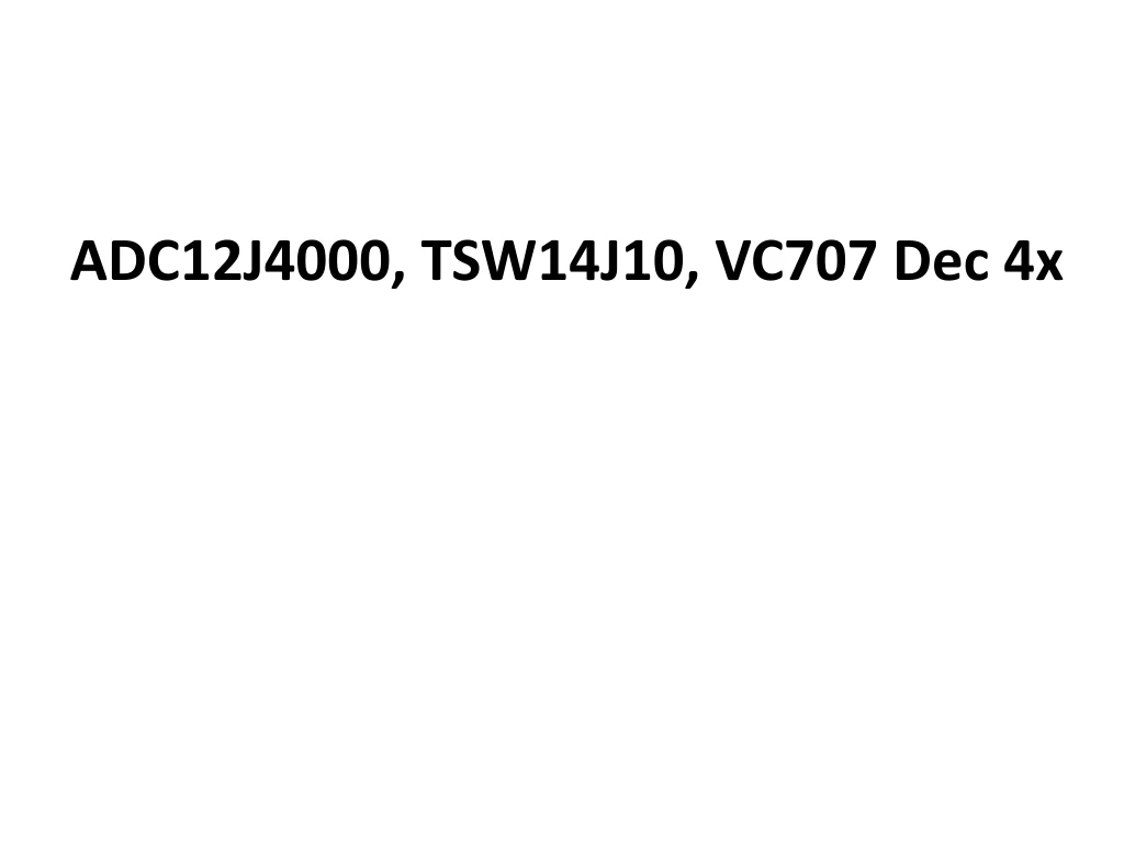
ADC12J4000, TSW14J10, VC707 Dec 4x. Test Setup: Single tone is given as input to the device. Test conditions: Fs = internal 4GHz Fin = 60 0MHz Dec 4 P54 mode LMK = 2GHz, clock dist mode VC707 Ref clock = 500MHz (/4 for LMK) VC707 Core clock = 250MHz (/8 for LMK) Lane Rate = 10G

E N D
Test Setup: • Single tone is given as input to the device. • Test conditions: • Fs = internal 4GHz • Fin = 600MHz • Dec 4 P54 mode • LMK = 2GHz, clock dist mode • VC707 Ref clock = 500MHz (/4 for LMK) • VC707 Core clock = 250MHz (/8 for LMK) • Lane Rate = 10G • V2p8 firmware
On ADC GUI, load the Preset 0 Frequency value as shown below
In Low Level View tab, set LMK04828 address 0x110 to 0x04 to set VC707 REFCLK = 500MHz
In Low Level View tab, set LMK04828 address 0x100 to 0x08 for VC707 Core CLK = 250MHz
Open HSDCD Pro, select “ADC12J4000_D4_DDR”, Enter “1G” for ADC Output Data Rate