Download
1 / 6
60 likes | 310 Views
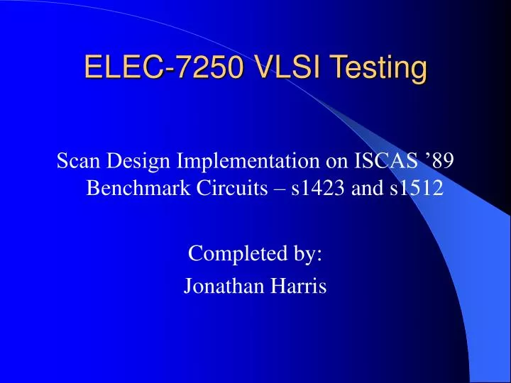
ELEC-7250 VLSI Testing. Scan Design Implementation on ISCAS ’89 Benchmark Circuits – s1423 and s1512 Completed by: Jonathan Harris. PI’s. PO’s. Combinational Logic. Scan In. PO or Scan Out. O 1. dff 1. dff 2. dff n. D Q. D Q. D Q. O 1. O 1. O 1. Clock. Scan Mode.

E N D
ELEC-7250 VLSI Testing Scan Design Implementation on ISCAS ’89 Benchmark Circuits – s1423 and s1512 Completed by: Jonathan Harris
PI’s PO’s Combinational Logic Scan In PO or Scan Out O 1 dff1 dff2 dffn D Q D Q D Q O 1 O 1 O 1 Clock Scan Mode What is Scan Design? 00110011 00101011
Disadvantages Gate and area overhead Performance penalty – 2 gate delays Long test application time Advantages High Fault Coverage Minimal Test Generation Time Easily Automated Scan Design – Pros & Cons