Download
1 / 17
170 likes | 278 Views
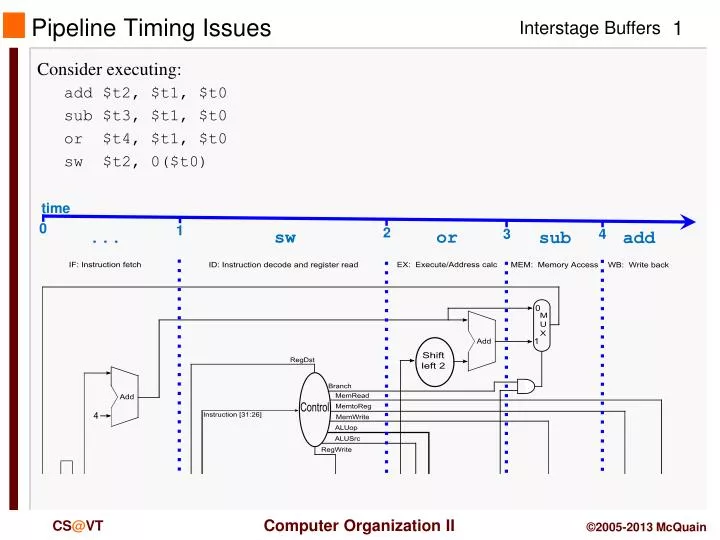
Pipeline Timing Issues. Consider executing: add $t2, $t1, $t0 sub $t3, $t1, $t0 or $t4, $t1, $t0 sw $t2, 0($t0). time. 0. 1. 2. 3. 4. . sw. or. add. sub. Pipeline Timing Issues. What happens during cycle 1? Among other things…

E N D
Pipeline Timing Issues • Consider executing: • add $t2, $t1, $t0 • sub $t3, $t1, $t0 • or $t4, $t1, $t0 • sw $t2, 0($t0) time 0 1 2 3 4 ... sw or add sub
Pipeline Timing Issues • What happens during cycle 1? Among other things… • - swreaches the ID stage, and Control sets MemWrite to 1 • - so, a memory write will occur while sub is in the MEM stage • - and that’s bad news… time 0 1 2 3 4 ... sw or add sub
Pipeline Timing Issues • What needs to happen instead? • - the value of MemWrite that goes with sw… • - … needs to travel forward, stage to stage as sw does time 0 1 2 3 4 ... sw or add sub time 0 1 2 3 4 ... ... sw sub or
Pipeline Timing Issues • What needs to happen instead? • - the value of MemWrite that goes with sw… • - … needs to travel forward, stage to stage as sw does time 0 1 2 3 4 ... ... ... or sw • So how do we make this happen?
Adding Buffers • Put storage buffers between adjacent stages: • Control writes/reads with the clock signal. • Write values exiting a stage to the “outbound” buffer. • Read values entering a stage from the “inbound” buffer. • So no signal (or data value) arrives before its time…
Pipeline Operation • Cycle-by-cycle flow of instructions through the pipelined datapath • “Single-clock-cycle” pipeline diagram • Shows pipeline usage in a single cycle • Highlight resources used • c.f. “multi-clock-cycle” diagram • Graph of operation over time • We’ll look at “single-clock-cycle” diagrams for load & store
IF for Load, Store, … PC+4 is computed, stored back into the PC, stored in the IF/ID buffer although it will not be needed in a later stage for LW or SW Instruction word is fetched from memory, and stored in the IF/ID buffer because it will be needed in the next stage. Write into the buffer
ID for Load Bits of load instruction are taken from IF/ID buffer, while new instruction is being fetched back in stage 1. PC+4 is passed forward to ID/EX buffer... Read register #1 and #2 contents are fetched and stored in ID/EX buffer until needed in next stage… #2 won't be needed. 16-bit field is fetched from IF/ID buffer, then sign-extended, then stored in the ID/EX buffer for use in a later stage. Read from the buffer
EX for Load PC+4 is taken from ID/EX buffer and added to branch offset… Computed branch target address is stored in EX/MEM buffer to await decision in next stage... but won't be needed. Read register #1 contents are taken from ID/EX buffer and provided to ALU. 16-bit literal is provided to ALU as second operand ALU result and Zero line are stored in EX/MEM buffer for use as memory address in next stage. Read register #2 is passed forward to EX/MEM buffer, for possible use in later stage… but won't be needed.
MEM for Load Zero line taken from EX/MEM buffer for branch control logic in this stage… Value on Read data port of data memory is stored in MEM/WB buffer, awaiting decision in last stage.. ALU result is taken from EX/MEM buffer and passed to Address port of data memory. ALU result also stored in MEM/WB buffer for possible use in last stage… Read register #2 contents taken from EX/MEM buffer and passed to Write data port of data memory.
WB for Load But the Write register port is now seeing the register number from a different, later instruction. Since load instruction, value from data memory is selected and passed back to register file.
Corrected Datapath for Load So we fix the register number problem by passing the Write register # from the load instruction through the various inter-stage buffers… …and then back, on the correct clock cycle.
EX for Store Almost the same as for LW… Read register #2 is passed forward to EX/MEM buffer, for use in later stage… for SW this will be needed.
MEM for Store Zero line taken from EX/MEM buffer for branch control logic in this stage… Value on Read data port of data memory is stored in MEM/WB buffer, awaiting decision in last stage.. ALU result is taken from EX/MEM buffer and passed to Address port of data memory. ALU result also stored in MEM/WB buffer for possible use in last stage… Read register #2 contents taken from EX/MEM buffer and passed to Write data port of data memory.
WB for Store Since SW instruction, neither value will be written to the register file… doesn't really matter which value we send back…
Questions to Ponder Can you repeat this analysis for other sorts of instructions, identifying in each stage what's relevant and what's not? How much storage space does each interstage buffer need? Why? Do the interstage buffers have any effect on the overall time required for an instruction to migrate through the pipeline? Why?
Summary Here’s our final configuration for the buffers: