Download
1 / 14
140 likes | 359 Views
Latch-TDC. Da-Shung Su Su-Yin Wang, Jia -Ye Chen Ting- Hua Chang, Wen -Chen Chang 2011/06/08. The Drift Time of Hits. 20 ns. RF. Tmax . drift = 1-2 s, depending on the gas used for the proportional tubes. Timing Relations Between Hits and Trigger. RF. “Latch”-TDC.

E N D
Latch-TDC Da-ShungSu Su-Yin Wang, Jia-Ye Chen Ting-HuaChang, Wen-Chen Chang 2011/06/08
The Drift Time of Hits 20 ns RF Tmax. drift = 1-2 s, depending on the gas used for the proportional tubes.
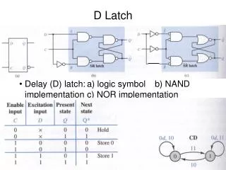
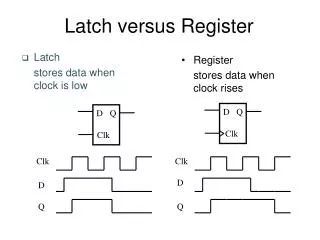
“Latch”-TDC • Each channel consists of a shift register with a depth longer than 64 clocks. Whenever there comes a wire chamber signal, a hit is registered. The actual depth of the shift register is determined by the need of trigger latency. • The signal of one channel will be sampled by the clock with four different phases and be placed in four shift registers respectively. We use both rising and falling edges of the clock for the sampling. The final timing resolution of sampling will be in principle 1/8 of the period of clock source. • The hit pattern sampled by four PLLs is represented by 4 bits for each channel, as shown in the table. • Upon the arrival of a trigger, the hit pattern of an accepted window of 64-step width in the shift register, 64*4=256 bits=32 bytes, will be copied to the output memory for each channel. This CIP action introduces the dead time of TDC module. • The timing information could be retrieved from the "position" of the hit in the shift register and the preset delay time. Multi-hit information is also preserved.
Sampling Results and Output • At each time bin, Q0, Q1, Q2 and Q3 are the sampling results of the input signal with the four different phases of the clock. • Q0 is the starting phase, i.e. t(Q0) is earlier those of the others. • “x” stands for either 0 or 1. • We assume that two hits are separated from each other more than 1 clock away, and a valid hit sustains more than 1-clock wide. No signal Leading edge detected. Signal on. Trailing edge detected.
Data Throughput • Assume each channel will output 32 bytes per event • For each card: 32*64 = 2048 bytes per event • For a more-full VME crate: 2048*15 ~ 30K bytes per event • For the system of total of 100 cards: 200KB per event • Assume Trigger rate 2KHz : 2000* 200 = 400 MB per sec • A Gigabit Ethernet support at 1 Gbps (1000 Mbps=125 MBps) is preferred. • If zero suppression is implemented, the data rate can be further reduced, perhaps by a factor of 2 or 3.
David Christian’s comments This sounds like a very good idea. I suggest using slightly wider time bins for the first two options... 2.5ns & 5ns rather than 2ns & 4ns. If we use slow gas, with average drift velocity ~ 40 microns/ns = .04mm/ns, then the maximum drift time in station 2 (~10mm drift) will be about 10/.04 = 250ns. This will be difficult to fit into a 256ns time window, but easy to fit into a 320ns time window. The resolution will still be pretty good, since (sigma=bin/root(12)) 5ns/root(12) = 1.44ns, which corresponds to ~60 microns at 40 microns/ns. If we use fast gas, with ave drift velocity 80-100 microns/ns, we may be able to use 64 2.5ns bins even for Stations 2 & 3 (& still have a contribution to the measurement error from TDC binning < 100 microns)... If the drift velocity is 100 microns/ns & we have to use 5ns bins, the TDC binning error would still be only 500u/root(12) ~ 150 microns. I'm not sure what the maximum drift time in the station 4 chambers is going to be... Ming measured 2.3 microseconds using Ar/C02 (80/20). If we have only 3 options of time bin width, I think the third option should give us a time window of about 2.5 usec. 64 bins each 40ns wide would give 2.56usec. That gets my vote.
Ting-Hua Chang’s Comments Regarding the maximum delay time, assume at t0 the particle hit H1 hodo, the TDC stop goes into the TDC module will be ~t0+1100 ns (using 350ns for 1 layer of V1495), while the signals from chamber will be t0+ TOF(ranging from 0 to 50ns ) + ~100 ns cable + drift time. So the maximum delay time should be increased for ST 1, and very marginal for station 2 & 3. We will need to increase the maximum delay to or provide an time window offset of ~1000 ns in the final version.
Current Design Specification I Frequency of clock source: 100 MHz
Current Design Specification II • Width of accepted window: 64 time bins. • Depth of shift register: 128 time bins. • The start time of the accepted window (or the relative position of the accepted window in the shift register) can be controlled via a register value set by the user. The value is from 0 to 64 with a step of 2. • For the purpose of zero suppression, we are considering setting up a flag bit in the register if all bits for 64 channels are all ZERO.
CSR2 0x0c (32 bits) Trigger Timing (Read) Delay Time CSR2 Time window (64 clocks) Gate (128 clocks)
Data structure for one time bin 1st 32-bit data 2nd 32-bit data ….. 7th 32-bit data 8th 32-bit data