Download
1 / 27
400 likes | 1.56k Views
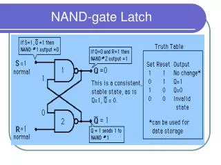
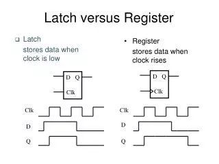
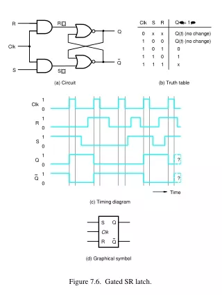
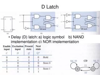
D Latch. Delay (D) latch: a) logic symbol b) NAND implementation c) NOR implementation. D Latch. The D latch is “transparent” As long as C=1, changes in D are propagated to the output D latch timing diagram. D Latch. D latch timing constraints Latches undesirable in a sequential machine

E N D
D Latch • Delay (D) latch: a) logic symbol b) NAND implementation c) NOR implementation
D Latch • The D latch is “transparent” • As long as C=1, changes in D are propagated to the output • D latch timing diagram
D Latch D latch timing constraints • Latches undesirable in a sequential machine • Why?
D latch • Logic function Q* = f(C,D,Q) = ? • Q* = DC + D’’Q + C’Q = CD + C’Q + DQ = CD + C’Q • Undesirable in sequential machines, because transparent • What does it imply for the sequential machine function?
Flip-flops • Flip-flops are pulse-triggered • Master-slave gated SR flip-flops • Symbol signifies rising pulse edge triggered
Master-slave gated SR flip-flop • Timing diagram • Master and slave alternate
Master-slave gated SR flip-flop • Timing diagram • Setup and hold times defined for the external inputs to the master latch • S and R must be stable around the clock edge that puts master on hold
Master-slave gated SR flip-flop • Excitation table (a) and Timing diagram (b) • Needs both the 0-1 and 1-0 transitions on C in order to operate properly • Logic function Q* = f(S,R,Q,C) = ?
Master-slave D flip-flop • Symbol signifies rising pulse edge triggered
Master-slave D flip-flop • Timing diagram • Needs both the 0-1 and 1-0 transitions on C in order to operate properly • Logic function Q* = f(D,Q,C) = ? • Q = D
Master-slave JK flip-flop • Same as SR flip-flop with J=S and K=R • When J=K=1, “toggles” state: Q*=Q’ • Why connect Q* to D of the same FF? Why not cascade 2 D Flip-flops? • Symbol signifies falling pulse edge triggered • Logic function Q* = f(D,Q,C) = ?
K Master-slave JK flip-flop • Has don’t cares • Q* = K’Q + JQ’
Master – Slave configuration • One way to avoid race-around conditions and transient oscillations • Needs both rising and falling clock edges to function correctly • Therefore known as “pulse triggered” circuits • Another way to avoid race-around and transients? • Design circuit that is sensitive to its excitation inputs only during rising or falling clock edge transitions • Called edge-triggered
G1 G2 G5 G6 G3 G4 Edge-triggered D flip-flop Rising edge triggered
G1 G2 G5 G6 G3 G4 Edge-triggered D flip-flop • Operation on Set • PRE’ = 0; CLR’ = 1 G5 = Q = 1; G1 = 1 • CLK = 0 G3 = 1 G6 = Q’ = 0 • CLK = 1 G2 = 0 G3 = 1 G6 = Q’ = 0 0 1 0 1 1 1 1 0 1 1 0 0 1 0 1 1 1
G1 G2 G5 G6 G3 G4 Edge-triggered D flip-flop • Operation on Reset • PRE’ = 1; CLR’ = 0 G6 = Q’ = 1; G2 = 1; G4 = 1 G5 = Q = 0 • CLR’ alone sets the outputs 1 1 1 0 0 1 1 0 1 1
G5 G6 Edge-triggered D flip-flop • Operation when both Set and Reset asserted • PRE’ = 0 G5 = Q = 1; G1 = 1 • CLR’ = 0 G6 = Q’ = 1; G2 = 1; G4 = 1 • Both Q and Q’ are 1 at the same time • No oscillation 0 G1 1 1 0 1 0 1 1 G2 0 1 1 G3 0 1 G4
Edge-triggered D flip-flop • Normal operation: PRE’ and CLR’ = 1 • Equivalent circuit without them • CLK = 0 G2 = G3 = 1 • G5 and G6 form a stable pair of cross-coupled inverters • Stable (hold) state G1 1 G2 G5 1 1 G6 0 G3 1 G4
Edge-triggered D flip-flop • Normal operation: PRE’ and CLR’ = 1; latch 0 • CLK = 01; D = 0 • G3 becomes 0 and sets the G5 G6 pair to 0 1 • CLK = 1; D = 01; G3 is still 0, G4 cannot change: no change. 1 G1 0 1 0 0 111 G2 G5 1 G6 01 G3 1 100 111 G4 01
Edge-triggered D flip-flop • Normal operation: PRE’ and CLR’ = 1; latch 1 • CLK = 01; D = 1 • G2 becomes 0 and sets the G5 G6 pair to 1 0 • CLK = 1; D =01; G2 is still 0, G3 cannot change; no change. 001 G1 111 1 100 G2 G5 01 G6 111 01 G3 0 001 G4 10 001
Edge-triggered D flip-flop • Timing specifications of SN7474, edge-triggered D FF • Delays from C to output are small • Value from D is almost instantlytransferred to Q
Edge-triggered JK flip-flops SN74LS73 is negative edge triggered
Edge-triggered JK flip-flops • SN74111 is a master-slave JK flip-flop with a positive edge-triggered master and negative edge pulse-triggered slave • Master flip-flop latches data on the rising edge of the clock and ignores it at other times • Slave transfers new value from master on falling clock edge
Edge-triggered T flip-flops • T (or Toggle, or Trigger) flip-flop • JK flip-flop in toggle mode • Negative edge-triggered: • Excitation table andstate diagram:
Clocked T flip-flops • Clocked T flip-flop • Changes on clock when T • Negative edge-triggered: • Excitation table, logic symbol andtiming diagram:
Edge-triggered versus pulse-triggered • Pulse triggered • Denoted by Q or Q on the output pin • Requires both edges of the clock before input values are transferred to and held at the output • Example: master-slave configuration • Edge triggered • Denoted by ¨ or o¨ on the clock pin • Input value transferred and held in response to a single rising or falling edge • Example: edge triggered D and JK flip-flops
Latches and flip-flops summary • Latches: • When data is to be captured from a signal line and stored • Flip-flops: • Used to remember state in sequential circuit design